Home
|
Introduction
Our device that we have designed operates in two modes. The first works as a basic GPS logger, which records GPS position information at timed intervals. The second mode only records position information when triggered manually over a wireless interface by an external device. The data is stored to an SD card, which can be removed for viewing the data on a computer. This can then be used with programs like Google Earth to display a map of the route traveled over the logging period, or in the case of using the external trigger with a camera, to correlate pictures with location information.
Inspiration With GPS technologies becoming much more affordable and available these days, there are many new applications to which it can be applied. One particular application that interested us was logging location data, especially with respect to photography. Geotagging is the process of adding location information to the metadata of digital photographs. Web sites such as Flickr can use this information to display such photographs on an interactive map. Having taken thousands of photographs over the past couple of years, on trips such as Jeff’s travels around Australia and New Zealand, this type of technology would be very helpful in organizing all of this information. Some expensive cameras include this functionality, but most do not. In those cases, a log of position information over time could be correlated against the time stamps on the photographs to add this information after the fact.
|
High Level Design
Hardware Design
|
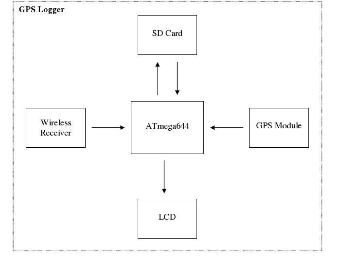
The hardware for
our design is comprised of the following:
ATmega644 Prototype Board
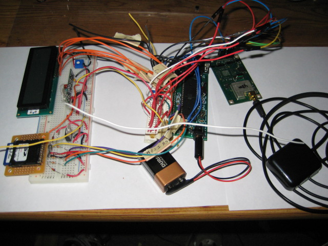
The ATmega644 is responsible for coordinating data flow between all of the other hardware components. We built the prototype board to use the ATmega644 on, and also attached the MAX233 and RS232 serial port connector to use for debugging purposes. We also used the LED on the prototype board as a helpful tool to blink every time we wrote GPS data to the SD card. The one thing that we changed with the board was to replace the LM340LAZ-5 voltage regulator with the LM340-T5 voltage regulator. We did this because the output current on the LM340LAZ-5 was only 100mA, and we needed more than that for the GPS receiver. The LM340-T5 fixed this issue because it has an output current of 1A, which was sufficient to run our GPS receiver with.
We used the transmit and receive jumpers on the prototype board to switch back and forth between receiving data from the GPS simulator through the serial port, and receiving data from our actual GPS receiver with the output of the receiver connected directly to the receive pin. Doing this allowed us to still use the transmit pin to send debugging information through the serial port to HyperTerminal.
To make our device portable, we obtained a battery to DC supply plug, and a 9V battery clip so that we could power our prototype board off of a 9V battery. This battery supply also powers the GPS receiver, SD card, LCD, and RCR-433 receiver through their interfacing with the prototype board. Through testing, we’ve found that the battery life on a 9V battery with our circuit is about 3 hours of operation. Navman Jupiter 12 GPS Receiver
The Navman Jupiter 12 is a 12-channel single board GPS receiver. This means that it’s capable of simultaneously tracking up to 12 visible satellites. The receiver can be powered from 3.3V to 5V, but we chose to power it with a 5V supply to ease interfacing with the ATmega644 and prototype board. Our particular receiver was part of the TU35-D420 series, which includes dead reckoning functionality. None of the dead reckoning functionality of this receiver was used.
The master reset line is tied high through a 57kΩ resistor as specified in the data sheet. The GPIO3 is similarly tied high to enable the module’s EEPROM for receiver settings rather than using the factory defaults. We connected the SDO1 output pin from the receiver to Pin D0, which is the uart receive pin, on the ATmega644.
The receiver has an OSX/MCX connector for an antenna. The receiver supports both passive and active antennas, with an optional preamplifier for active antennas. The datasheet specified that a current limiting circuit was required if the preamplifier was used to prevent more than 100mA from passing through the preamplifier in the event of a short circuit. This was accomplished using two parallel 75Ω resistors on the power input to the preamplifier.
The antenna that we chose to use was an active GPS antenna at the L1 frequency of 1575.42 MHz. It can be powered from 3.0 to 5.0 V, and has a gain of approximately 30 dBi. We chose this antenna due to its high gain, low price, and availability.
SD Card and Socket
We chose to interface our SD card in SPI mode with the MCU. To implement our SD card hardware, we sampled an SD card socket from Molex. The majority of the hardware design involved for it was to implement an effective level shifter between the ATmega644’s Port B pins that we used and the SD card. The SD card runs at 3.3V, so we powered it using a LM1117T-3.3 voltage regulator. We then needed to level shift all of the data from the output pins of the MCU to the inputs of the SD card from 5V to 3.3V. The three SD card inputs that needed this were the chip select, data in, and clock. We accomplished this by using a 1kΩ series resistor between the MCU and SD card inputs, along with a clamping diode from the SD card inputs to the 3.3V Vcc. The data out pin of the SD card was connected to the MISO input to the MCU. We also put a 57kΩ pull-up resistor between the data out pin of the SD card and the 3.3V Vcc as recommended by the SD specification. LCD
We used a standard 16 character, 2 line LCD to display the GPS latitude and longitude coordinates at all times while the GPS logger is on. We control the contrast with a 10k trimpot, and interface the LCD through Port C of the ATmega644. Radiotronix RCT-433 Transmitter
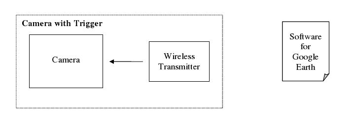
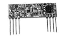
To implement the wireless trigger capability of our GPS logger, we used the Radiotronix RCT-433 Transmitter and RCR-433 Receiver. We chose to use them due to their low cost, simplicity, and availability in the lab. They operate at a center frequency of 433.92 MHz.
We designed a separate hardware circuit for the transmitter to function as the trigger for our device, and interface with the camera. We wanted the circuit to be as simple as possible, and avoid needing another MCU on the transmitter side. The transmitter can operate between 1.5V and 12V. For portability, we chose to run it off of a 9V battery, so we used another 9V battery clip in the circuit for our transmitter. We connected the 9V battery to an LM340LAZ-5 voltage regulator so that we could run this circuit off of a 5V Vcc. This was not necessary for the RCT-433 as it could run off of 9V as well, but since the trigger also interfaces with our camera, which shouldn’t have more than 5V on the USB input, this design was chosen.
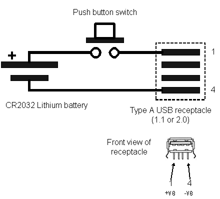
We connected a 10 inch wire antenna to the antenna output of the RCT-433, which worked well for our transmission needs. We connected a push button between the Vcc and data inputs to the transmitter so that we could transmit a short pulse to the receiver when we wanted to trigger our GPS logger. Since the transmitter uses on-off keying (OOK), these pulses would be relatively easy to detect be the receiver. We also connected a 10kΩ resistor between the data input to the transmitter and ground so that there is not a short when the push button is pressed. Lastly, we connected the data input pin of the transmitter to the USB cable which we used to interface with our camera, so that when we pushed the button to trigger our GPS logger it would also take a picture with the camera. Radiotronix RCR-433 Receiver
The RCR-433 receiver operates at 5V, so we powered it off of our 5V Vcc used for the prototype board. We also inserted a 0.01μF capacitor between Vcc and ground to eliminate some of the noise from the power supply from interfering with our signal received. We connected another 10 inch wire antenna to the antenna input of the receiver to receive our trigger pulses from the transmitter.
Initially, we looked at using the digital data output from the receiver to interface with the MCU, but the signal was a very noisy square wave, and appeared to require a bit of work to detect our trigger pulses, which just widened the period of the square wave. So, instead we chose to use the analog output from the receiver. This was a noisy signal centered around 2.5V, which spiked when we pressed the trigger button on the transmitter. To make this more detectable by the MCU, we placed a 0.01μF capacitor in series between the analog output of the receiver and Pin B2 of the ATmega644. The eliminated the DC bias from the signal, so that the signal going into the MCU had small noise variations and was centered at 0V. When the transmitter button was pressed, this signal would spike to about 4V for a brief period of time before returning to 0V. This spike was detected by connecting the output to the positive input of the voltage comparator on the MCU (Pin B2). A reference voltage, determined by a 10k trimpot, was connected to the negative input of the voltage comparator (Pin B3). We were able to adjust the trimpot voltage level to eliminate noise from triggering our device, but still allow our transmitter circuit to break the threshold and trigger it.
Camera
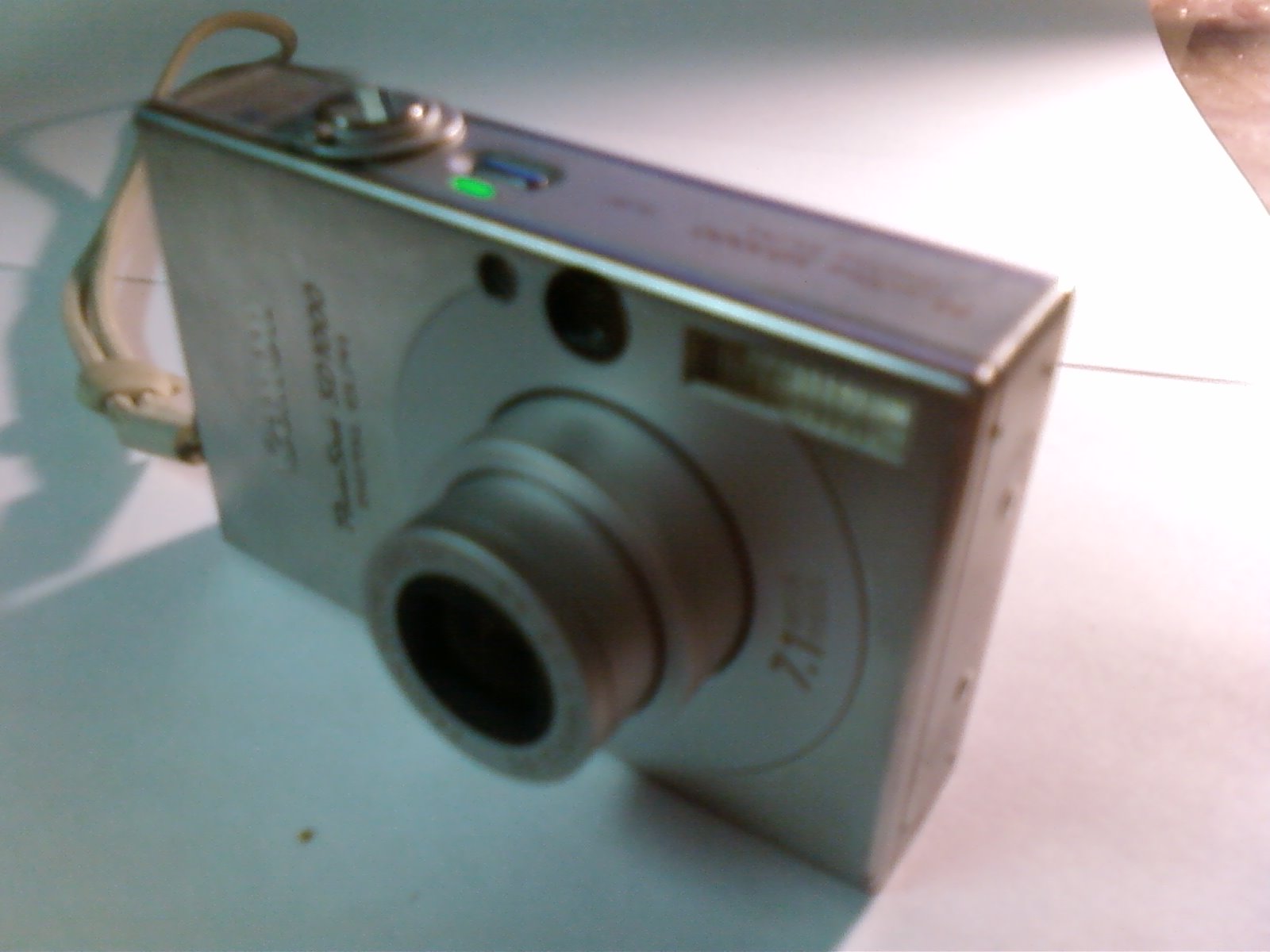
The camera used was a Canon PowerShot SD1000, loaded with the CHDK firmware add-on. CHDK adds many features not typically available on this camera. The relevant feature for this project was the ability to create a remote shutter release. When enabled, the camera will take a picture if between 3 and 5V are applied between pins 1 and 4 of the USB connector. We were able to implement this by connecting it to our push button trigger described previously.
|
Software Design
|
The software for our design is comprised of the following:
NMEA Parsing
The GPS receiver can output data in the standard NMEA 0183 ASCII format or a manufacturer proprietary binary format. The binary format provides more information, but NMEA is easier to parse the needed information for this application, and is more compatible with desktop applications. For this application, we record three types of NMEA messages: GGA, GSA, and RMC. Examples of each of these follow: $GPGGA,204542,4226.3744,N,07629.1623,W,1,03,4.36,229.5,M,-33.9,M,,*45 For more information on the formatting of NMEA sentences, please see the References page Each message begins with a $ sign, and ends with a \r\n, with a maximum length of 80 characters which eases parsing. Since each of these messages is sent once a second by the GPS module, we implemented an interrupt-driven uart receiver that places each received byte into a circular buffer. To maintain concurrency, messages are parsed out of this buffer by a task that executes every 500 milliseconds. This task stores the most recent copy of the GGA, GSA, and RMC messages, as well as extracting the current data and time, as well as the status of the GPS fix. The status of the GPS fix is determined by the fix quality parameter of the GGA sentence.
For our initial testing of the parsing code, we used a GPS simulator called gpsfeed+, which outputs varying GPS location data on the serial port of the computer. This was then run through our uart to the ATmega644 in place of the actual GPS receiver until our parsing testing was complete.
LCD Display
The LCD is updated every 500 milliseconds with the current position retrieved from the NMEA parser. This is displayed as “LAT: <position>” on the first line of the LCD, and “LON: <position>” on the second line of the LCD. If the GPS receiver does not currently have a GPS fix, then “NO GPS FIX” is displayed on the LCD instead.
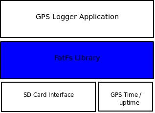
For ease of use, we wanted the logger to support writing and reading SD cards using the FAT file system. This is the standard file system used by most removable media today. We found a library called FatFs designed for this purpose on a variety of microcontrollers. FatFs is free software with no restrictions on usage. It is designed with a hardware abstraction layer so that it can be easily adapted to different hardware configurations.
For this application, the disk interface is the SD card controlled over an SPI interface. SD cards typically operate using SPI mode 0. This means that the ATmega644 is the SPI master, with CPOL = 0, and CPHA = 0. Although the SD card supports a SPI interface, this is not the default interface when the card is powered on. To initialize the card, we set the SPI clock rate to a slow speed of 125 kHz, and apply 80 dummy clock cycles by transmitting 0xFF 10 times. After this, the microcontroller sends CMD0 with /CS low to enter SPI mode in the idle state. Once in SPI mode, the card is initialized using ACMD41 repeatedly until the idle state bit in the response is cleared. At this point, the card is ready for read and write operations, which can be done at a higher clock rate. We used a clock rate of 1 MHz. This rate could have been increased, but performance was not very important due to the small amount of data being read or written in a given period of time.
FatFs included a sample implementation of an SD card interface for AVR microcontrollers. This sample implementation did not initially work with our microcontroller. The SPI configuration, power management, initialization, and disk timer were all modified to work with our hardware. The disk timer also required modification to be driven by our central 1 millisecond interrupt-driven scheduler. We also implemented the real time clock from scratch. If a GPS fix is available, the current date and time is obtained from the NMEA module. Otherwise, an approximation is made based on the current up time of the logger. This clock is responsible for the time stamps on files written to the SD card.
File access is provided by FatFs functions that are analogous to standard C file functions (e.g. f_open vs. fopen). Prior to opening any file, a file system object must be created to reference the drive. Both this and file operations are simplified by the fact that the hardware interface code only supports one disk.
Configuration Options
During power-up, the file gps_set.txt is read from the SD card to determine configuration options. If the word “trigger” appears at the beginning of a line, wireless triggering will be enabled. If the word “interval” appears at the beginning of a line, interval logging will be enabled. The interval is defined in seconds, and is separated by a space after the word “interval” in the line. Both modes can be enabled simultaneously. If the file can not be read, both modes are enabled by default, with a 30 second interval.
Trigger and Log Writing
Upon power-up, the logger will create a file of the form gps_xxx.txt, where xxx is the lowest number from 000 to 999 that does not currently exist. Log writing is initiated by asserting the writeFlag variable. The writeFlag is asserted by the trigger process, and/or at the specified time interval, depending on the configuration. After the flag is asserted, the most recent GGA, GSA, and RMC sentences are written to the SD card. After writing the data, the file system is synchronized to prevent data loss if the logger is turned off in between writes. The LED is illuminated while data is being written both as an indicator and as a warning not to turn off the logger.
The trigger is implemented using the analog compare interrupt on the ATmega644. The interrupt is set to fire on the rising edge of the analog comparator output, which represents the received RF signal crossing the voltage threshold. The interrupt service routine will assert writeFlag if trigger mode is enabled, and the interrupt has not occurred in the last second. This 1 second delay between allowable interrupts was put into the code for trigger debouncing purposes. It is unlikely to receive more than one genuine trigger per second in this application because of delay in the camera.
We chose to use a single on pulse as our trigger to greatly simplify our hardware needed to implement our wireless RF trigger. This resulted in it being more susceptible to noise since we used this instead of any specific data sequence for triggering. However, this was an acceptable trade off for our design since we wanted our transmitting circuit to be very small so that it could interface easily with the camera.
Google Earth Interface
Correlating picture and position data was performed using free software known as GPicSync. This software takes an NMEA log file from the logger, and a folder full of pictures. It determines the location of each picture by using the GPS location that is closest in time to the given picture. Our triggering mode allows this difference in time to be very small. GPicSync also generates a KMZ file, which includes the path taken with photothumbnails overlaid in the appropriate places. KMZ files can be opened using Google Earth. GPicSync also supports exporting this information in a Google Maps format that can be embedded in a website.
We also used the website http://www.gpsvisualizer.com/. This website allows the user to upload a GPS file, and then choose an output format such as Google Earth or Google Maps to display the route of the coordinates taken on it. This is a simpler method than GPicSync if the user is solely interested in using the logging mode of our GPS logger, and seeing the routes that were travelled. |
Results
|
Our GPS logger worked satisfactorily
during our testing. We were able to record the GPS data to an SD
card, and use that data to geotag photos taken during a walk around
Cornell’s campus.
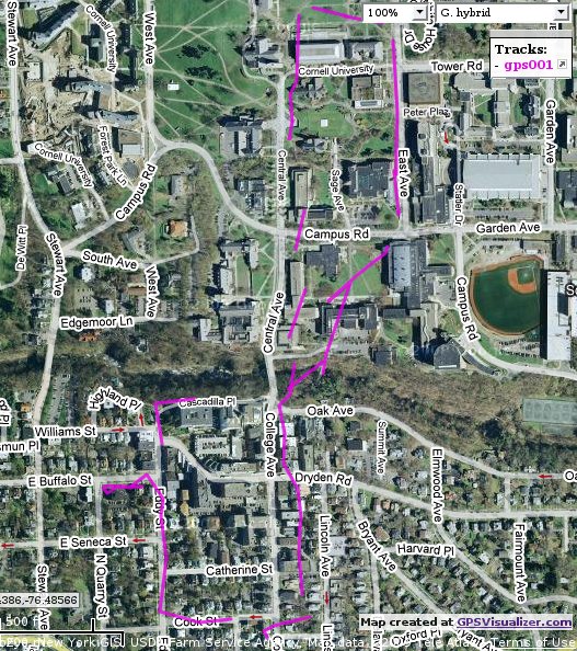
The following is the map from Google Maps obtained by uploading our GPS file onto the website gpsvisualizer: The following is the interactive map with photothumbnails of our pictures overlaid, obtained using GPicSync: The accuracy seen in our GPS location information was typical of a non-WAAS GPS receiver, which is on the order of tens of meters. The integration of the various components in our design worked very well, without any concurrency or hesitation issues. Human factors and usability for our design are not a large consideration because most of its operation is autonomous, and then the data is processed elsewhere. The configuration and data processing tools could be completed in various applications that could have interfaces tailored to their purpose or users. This includes users with any special needs. |
Conclusion
|
Overall, we were very happy with the results of our project. It met all of our specifications that we had generated in our original project proposal. Originally, we had discussed with our T.A. about how we may need to get rid of the wireless trigger part due to time limitations and the complexity of other parts of the design, but we ended up having enough time to be able to get this implemented as well.
We were slightly disappointed in the performance of the GPS receiver itself. Signal acquisition was more difficult than it should have been. Several times we had to attach the antenna to something metal in order to get the initial GPS fix. Even in this situation, it often took more than 2 minutes to obtain a fix, although this time could have been shortened by using a backup battery to maintain almanac and time information. It is possible that the performance issues were related to the quality of our antenna, which was of questionable origin. The antenna current limiting circuit may also have negative effects on the antenna performance. To improve this design, a higher end GPS receiver and antenna would be needed, which were out of the budget constraints for this project.
Our implementation of the wireless trigger (using the RCR-433 receiver) was very sensitive to false positives from noise, especially in the 433 MHz band, since we only look at the amplitude of the signal rather than any specific data sequence. In the lab, this wasn’t a problem except for when other groups were using RF broadcasting as well. However, when we took our device outside, we encountered a lot more false triggers from noise. We were able to practically eliminate these false triggers by increasing the reference voltage threshold from the trimpot to be greater than the noise level, so this sensitivity was acceptable. Also, the range of the trigger worked well at least out to 10 feet with this new threshold level, which was satisfactory.
We would have preferred to have the camera initiate the wireless trigger on its own, rather that have an external shutter release that also activated the wireless trigger. However, we were unable to find an elegant way to determine when the shutter is pressed without hardware modifications to the camera.
|
Considerations
|
Applicable Standards
The GPS receiver that we used was a commercially available product for OEM applications, so it is reasonable to assume that it meets all relevant standards for its operation. Our RF transmitter is also a commercially available product. This implies that the transmitter complies with FCC rules for general usage. Since our application is atypical for this transmitter, its usage is governed as a periodic intentional radiator by Section 15.231 of the FCC Part-15 Rules for unlicensed RF devices. The circuitry of the transmitter ensures that the transmission length is within the rules of this section. Lastly, we believe that our SD card interface conforms to the specification from the SD Association.
Intellectual Property and Legal Considerations
The prototype board that we used for the ATmega644 was designed and laid out by ECE 476 Professor Bruce Land. The initial test code for the prototype board was also created by Bruce Land. The code used for uart and LCD interfaces was provided as part of earlier labs in ECE 476.
The FatFs file system library was used in compliance with its license. The Secure Digital memory cards are covered by multiple patents owned by the SD association. Some features, such as DRM and encryption, require licensing royalty fees. However, the card can be interfaced as an MMC card over an SPI interface without needing to pay any royalties. This interface is adequate for the needs of this device. All other code and circuitry was original. We do not believe that there are patent opportunities for this device because similar devices already exist.
Ethical Considerations
A large potential impact of this device involves ethical considerations. The increased information availability in all GPS systems brings many benefits, but also poses risks when that information is used improperly. These risks often invade on personal privacy. For example, such a device could be hidden in a car unknown to the driver for tracking purposes. However, no aspect of our design makes it particularly targeted for unethical use by end users.
Referring to the IEEE Code of Ethics, our project has no safety or health consequences to its users. The only environmental issue that needs to be considered is the proper disposal of empty batteries. There were no conflicts of interest regarding the completion of this project. No individual involved had any financial or professional benefit. We were honest and realistic in stating results based on our available data and observations. We researched the technologies that we used in depth ahead of time so that we could fully understand the use and potential consequences of them. While some of the technology we worked with was new to us, we did not exceed our experience level and limitations in working through the design. We have properly credited the contributions of others, particularly intellectual property. We are seeking constructive criticism on this project in the form of a grade, and comments during our final demo. We frequently helped colleagues that encountered issues similar to ones that we had seen previously, in particular with the interface with our GPS receiver module. |
Appendices
|
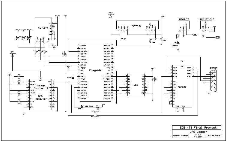
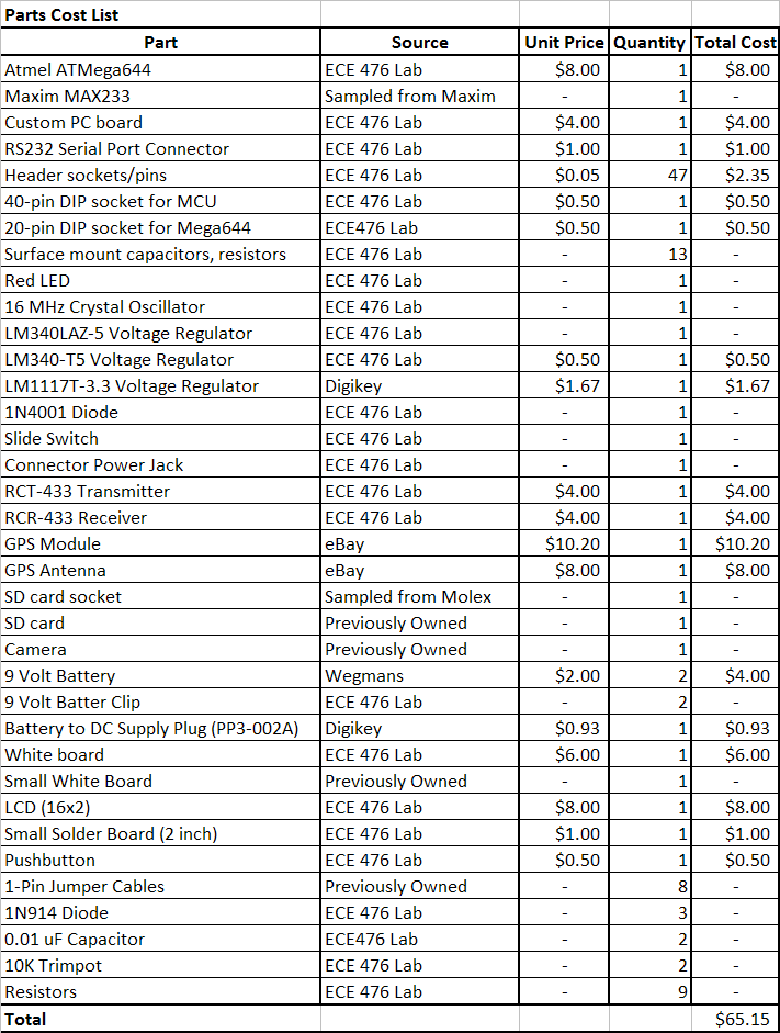
Acknowledgements We would like to especially thank Bruce Land for all of his help and miscellaneous tips along the way. We would also like to thank our T.A. Xi Guo for his help in lab throughout the semester. Finally, we would like to thank eBay for allowing us to complete this project within budget. We enjoyed the opportunity to complete a project on a topic that has been of interest to us for a long time. Appendix A: Source Code Full source code for this project is available for download here. Appendix B: Schematics Main circuit: Wireless Trigger Circuit: Note: USB pin 2 is actually pin 4. Schematics can also be downloaded in PDF and ExpressSCH format. Wireless Trigger Schematic: PDF SCH Appendix C: Budget and Parts List Our budget for this project was $75, and we were able to meet it with room to spare, with total costs of $65.15. We were able to keep our costs for this project down by purchasing the two most expensive parts, the GPS module and antenna, for $18.20 combined off of eBay. Normally, these two parts together will run over our entire budget. We also kept our costs lower by sampling a couple of the other parts, such as the SD card socket and MAX233. Appendix D: Distribution of Tasks Matthew Kuzdeba
Jeff Melville
|
References
|
Datasheets
Atmel ATMega 644 Microcontroller Navman Jupiter 12 GPS Receiver (TU35-D420-021) Secure Digital Card Product Manual Radiotronix RCR-433 RF Receiver Radiotronix RCT-433 RF Transmitter Maxim MAX233 RS-232 Driver/Receiver LM340LAZ-5: 5V Voltage Regulator (100mA) LM340-T5: 5V Voltage Regulator (1A) LM1117T-3.3-ND: 3.3V Voltage Regulator (800mA) Other Documents How to use SDC/MMC Zodiac GPS Receiver Family Designers Guide NMEA Data Circuit for a similar GPS receiver Utilized Libraries/Software FatFs - Microcontroller compatible R/W FAT12/16/32 library CHDK - Firmware add-on for Canon digital cameras gpsfeed+ - NMEA simulator used for indoors testing ECE 476 Website - UART and LCD libraries, previous labs GPSVisualizer - Quickly view GPS logs on a map GPicSync - Correlate photographs to GPS log and export to Google Earth / Maps Google Earth Vendors Digikey Jameco Maxim Molex |





_displayNameOrEmail_ - _time_ - Remove
_text_