DDA on FPGA
A modern Analog Computer
The Digital Differential Analyzer (DDA) is a device to directly compute the solution of differential equations. The DDA is a simulation of an analog computer, and is inherently parallel in operation. It can be mapped easily into an FPGA by defining mathematical integrators, adders, multipliers and other operations, then wiring them together to produce the desired dynamics. The system described here has an maximum integrator update rate of higher than 50 MHz, so it is possible to accurately simulate audio-rate signals.
For more background on analog computers see:
On this page you can follow these links to examples of DDAs applied to linear and nonlinear systems:
A summary of the second order system controlled by NiosII appeared in Circuit Cellar Magazine (manuscript).
The general approach using DDAs will be to simulate a system of first-order differential equations, which can be nonlinear. Analog computers use operational amplifiers to do mathematical integration. We will use digital summers and registers. For any set of differential equations with state variables v1 to vm:
dv1/dt = f1(t,v1,v2,v3,...vm)

dv2/dt = f2(t,v1,v2,v3,...vm)

dv3/dt = f3(t,v1,v2,v3,...vm)
...
dvm/dt = fm(...)
We will build the following circuitry to perform an Euler integration approximation to these equations in the form
v1(n+1) = v1(n) + dt*(f1(t,v1(n),v2(n),v3(n),...vm(n))

v2(n+1) = v2(n) + dt*(f2(t,v1(n),v2(n),v3(n),...vm(n))

v3(n+1) = v3(n) + dt*(f3(t,v1(n),v2(n),v3(n),...vm(n))

...

vm(n+1) = vm(n) + dt*(fm(...))
Where the variable values at time step n are updated to form the values at time step n+1. Each equation will require one integrator. The multiply may be replaced by a shift-right if dt is chosen to be a power of two. Most of the design complexity will be in calculating F(t,V(n)).
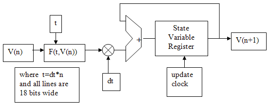
We also need a number representation. I chose 18-bit 2's complement with the binary point between bits 15 and 16 (with bit zero being the least significant). Bit 17 is the sign bit. The number range is thus -2.0 to +1.999985. This range fits well with the Audio codec which requires 16-bit 2's complement for output to the DAC. Conversion from the 18-bit to 16-bit just requires truncating the least significant two bits ([1:0]). A few numbers are shown in the table below. Note that the underscore character in the hexidecimal form is allowed in verilog to improve readability.
Decimal number |
18-bit 2's comp
representation
|
1.0 |
18'h1_0000 |
0.5 |
18'h0_8000 |
0.25 |
18'h0_4000 |
0 |
18'h0_0000 |
-0.25 |
18'h3_c000 |
-0.5 |
18'h3_8000 |
-1.0 |
18'h3_0000 |
-1.5 |
18'h2_8000 |
-2.0 |
18'h2_0000 |
Second order system (damped spring-mass oscillator):
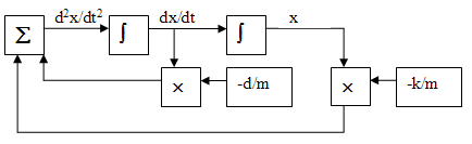
As an example, consider the linear, second-order differential equation resulting from a damped spring-mass system:
d2x/dt2 = -k/m*x-d/m*(dx/dt)
where k is the spring constant, d the damping coefficient, m the mass, and x the displacement. We will simulate this by converting the second-order system into a coupled first-order system. If we let v1=x and v2=dx/dt then the second order equation is equivalent to
dv1/dt = v2

  dv2/dt = -k/m*v1-d/m*v2
These equations can be solved by wiring together two integrators, two multipliers and an adder as shown below. In the past this would have been done by using operational amplifiers to compute each mathematical operation. Each integrator must be supplied with an initial condition.
Converting this diagram to Verilog, the top-level module verilog code defines the 18-bit, signed, state variables and a clock divider variable (count). The clocked section resets and updates the state variables. The combinatorial statements compute the Euler approximation to the F(t,V(n)). The separate multiply module ensures that the multiplies will be instantiated as hardware multipliers. The Audio_DAC_ADC module was modifed to allow either ADC-to-DAC passthru or to connect the computation output to the DAC, depending on the position of SW17. SW17 up connects the computation.
/state variables
reg signed [17:0] v1, v2 ;
wire signed [17:0] v1new, v2new ;
//signed mult output
wire signed [17:0] v1xK_M, v2xD_M ;
// the clock divider
reg [4:0] count;


//Update state variables of simulation of spring- mass
	always @ (posedge CLOCK_50)
	begin
		count <= count + 1;
		if (KEY[3]==0) //reset
		begin
			v1 <= 32'h10000 ; //
			v2 <= 32'h00000 ;
			//count <= 0;
		end
		else if (count==0)
		begin
			v1 <= v1new ;
			v2 <= v2new ;
		end
	end

	// Compute new F(t,v) with dt = 2>>9
	// v1(n+1) = v1(n) + dt*v2(n)
	assign v1new = v1 + (v2>>>9);
	// v2(n+1) = v2(n) + dt*(-k/m*v1(n) - d/m*v2(n))
	signed_mult K_M(v1xK_M, v1, 18'h10000);
	signed_mult D_M(v2xD_M, v2, 18'h00800);
	assign v2new = v2 - ((v1xK_M + v2xD_M)>>>9);

module signed_mult (out, a, b);
	output 		[17:0]	out;
	input 	signed	[17:0] 	a;
	input 	signed	[17:0] 	b;
	wire	signed	[17:0]	out;
	wire 	signed	[35:0]	mult_out;
	assign mult_out = a * b;
	assign out = {mult_out[35], mult_out[32:16]};
endmodule
Time scaling the solution requires consideration of the value of dt and the update rate (CLOCK_50/(clock divider)) of the state variables. As shown in the code, the clock divider variable (count) is 5-bits wide, so it will overflow and cause an update every 32 CLOCK_50 cycles. If the time step, dt=2-9, then 29 steps must equal one time unit. 29 steps at an update rate of 5*107/32 yields a time unit of 0.328 mSec. A k/m=1 implies a period of 6.28 time units per cycle, so one cycle in this case would be 2.06 mSec. corresponding to 486 Hz.
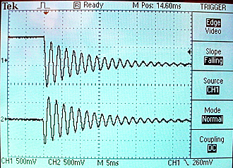
If the calculation is scaled in time to be in the audio range, then the audio DAC may be used to watch waveforms on an oscilloscope. For the damped spring-mass oscillator with a k/m=1, d/m=1/16, dt=2-8, and a clock rate of 5*108/64 I got the figure below. The top trace is v1 and the bottom is v2. The frequency computed from the time scaling considerations is 486 Hz, while the measured was 475 Hz. Reducing dt to dt=2-9 (see paragraph above) and the clock divider to 32 made the measured frequency 486, matching the computed value. The better match with smaller dt illustrates that the integration is approximate.
The whole project is zipped here. The design consumed 2% of the logic resources of the FPGA, 1% of the memory, and 4 out of 70 9-bit multipliers. You could threfore expect to put up to 50 integrators and 35 multipilers in a bigger design.
Driven second order system (IIR bandpass/lowpass filter)
Using a DDS system to drive the second order system with a sine wave yields a bandpass/lowpass filter depending on the damping coefficient. If the damping is small, the the system acts like a resonant filter. If the damping is 0.707, the system acts as a 2-pole Butterworth lowpass filter. The top-level module was modified to include a DDS sinewave generator with a frequency set by pushbutton KEY0. The core update code is shown below.
// dt = 2>>9
// v1(n+1) = v1(n) + dt*v2(n)
assign v1new = v1 + (v2>>>9)  ;
// v2(n+1) = v2(n) + dt*(-k/m*v1(n) - d/m*v2(n))
signed_mult K_M(v1xK_M, v1, 18'h1_0000);
signed_mult D_M(v2xD_M, v2, 18'h0_0800); //light damping
//scale the input so that it does not saturate at resonance
signed_mult Sine_gain(Sinput,{sine_out[15],sine_out[15],sine_out}, 18'h0_4000);
assign v2new = v2 - ((v1xK_M + v2xD_M )>>>9) + (Sinput>>>9) ;
Two mpegs of the scope screen show the low-damping (band pass) case for fast and slow frequency steps. The top trace is the input, and the bottom is the filter output. A sudden increase in output is seen near the resonant frequency of 485 Hz. If you stop the video at a frequency below the resonant frequency, you will see that the input and output are in phase. Above the resonant frequency, the phase is 180 degrees. The whole project is zipped here.
Second order system with higher Accuracy DDA.
For some dynamic systems, 18 bit accuracy is barely enough. Extending the accuracy to 27 bits seems to be a reasonable tradeoff between accuracy and the large increase in the number of required multipliers. The second order driven system increases from 6 multipliers to do 3 multiplies to 14 multipliers. Values for the 27-bit numbers with the binary-point between 24 and 23 are shown below.
Decimal number |
27-bit 2's comp
representation
|
2.99999 |
27'h2_FFFF_58 |
2.0 |
27'h2_0000_00 |
1.0 |
27'h1_0000_00 |
0.5 |
27'h0_8000_00 |
0.25 |
27'h0_4000_00 |
0 |
27'h0_0000_00 |
-0.25 |
27'h7_c000_00 |
-0.5 |
27'h7_8000_00 |
-1.0 |
27'h7_0000_00 |
-1.5 |
27'h6_8000_00 |
-2.0 |
27'h6_0000_00 |
-3.0 |
27'h5_0000_00 |
-4.0 |
27'h4_0000_00 |
The top-level module and multiply routine (shown below) were modified to accomodate the larger bit representations. The project for the second order driven system is zipped here.
//////////////////////////////////////////////////
//// signed mult of 3.24 format 2'comp////////////
//////////////////////////////////////////////////
module signed_mult (out, a, b);
	output 		[26:0]	out;
	input 	signed	[26:0] 	a;
	input 	signed	[26:0] 	b;
	wire	signed	[26:0]	out;
	wire 	signed	[53:0]	mult_out;
	assign mult_out = a * b;
	assign out = {mult_out[53], mult_out[50:24]};
endmodule
Second order system controlled by NiosII.
It is often useful to be able to control an analog computer using a digital computer. Such a system is called a hybrid computer. For example you might want to sequence through a set of input frequencies applied to the simulated system to build a Bode plot. A NiosII cpu was built on the FPGA with ports to (1) control the DDS frequency, (2) control the gain of the sinewave applied to a second order system, (3) control the analog reset and start the simulation, (4) record the amplitude and phase shift of the system under test. The top-level verilog module contains the DDA simulation of the second order system and the NiosII cpu. The GCC program running on the NiosII:
- Holds the DDA in reset, and initializes the test frequency
- Releases the DDA reset and waits 10 cycles of the test frequency
- Waits until the output phase and magnitude reach steady-state
- Prints the phase and magnitude
- Iincrements the frequency by a factor
- Repeats the above steps for a number of frequencies
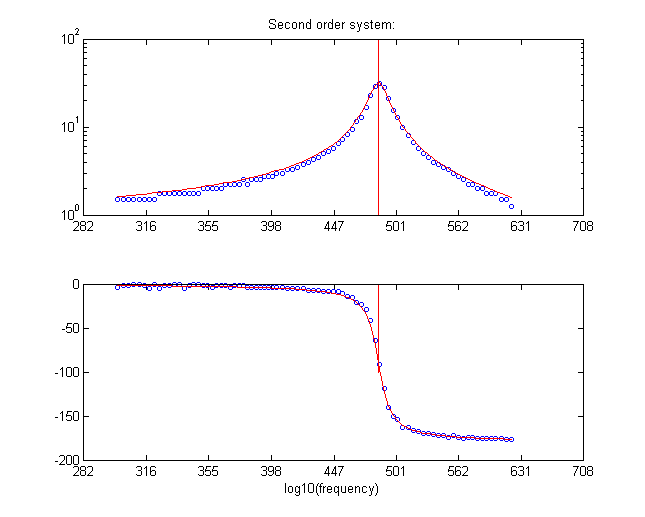
An mpeg of the frequency scan shown on an oscilloscope shows the input on the top trace and output on the bottom trace. You can easily see the dramatic increase in amplitude near resonance. You can also detect the phase shift. The results printed by the NiosII are available as text for a frequency sweep. The amplitude is in output/input ratio, phase is degrees. Note that the amplitude is not very accurate at low amplitudes because the input gain was not modulated, which causes quantization errors. The results are combined into a magnitude and phase plot with this matlab routine. The vertical red line indicates the computed resonant frequency for the linear system. the red curves are the analytical solution of a second order system with the same natural frequency and damping. The phase should be -90 degrees at the red line.
The whole project is zipped here.
Second order system with modularized integrator
A clearer version of the above project can be made by factoring the integration code into a separate module. The top-level module seems more like wiring an analog computer. A bit of the top-level module shows the wiring.
	// wire the integrators
	// time step: dt = 2>>9
	// v1(n+1) = v1(n) + dt*v2(n)
	integrator int1(v1, v2, 0,9,AnalogClock,AnalogReset);

	// v2(n+1) = v2(n) + dt*(-k/m*v1(n) - d/m*v2(n))
	signed_mult K_M(v1xK_M, v1, 18'h1_0000); //Mult by k/m
	signed_mult D_M(v2xD_M, v2, 18'h0_0800); //Mult by d/m
	//scale the input so that it does not saturate at resonance
	signed_mult Sine_gain(Sinput,{sine_out[15],sine_out[15],sine_out}, {2'h0,Sgain});
	integrator int2(v2, (-v1xK_M-v2xD_M+Sinput), 0,9,AnalogClock,AnalogReset);
The integrator module is
show below. The parameter order for the integrator is: state variable output, F(t,V(n)) input, initial value input, dt represented as the number of shift right bits, clock and reset. The state variable takes on the initial value when the reset input is zero.
/////////////////////////////////////////////////
//// integrator /////////////////////////////////
/////////////////////////////////////////////////
module integrator(out,funct,InitialOut,dt,clk,reset);
	output [17:0] out; 				//the state variable V
	input signed [17:0] funct;      //the dV/dt function
	input [3:0] dt ;				// in units of SHIFT-right
	input clk, reset;
	input signed [17:0] InitialOut; //the initial state variable V

	wire signed	[17:0] out, v1new ;
	reg signed	[17:0] v1 ;

	always @ (posedge clk)
	begin
		if (reset==0) //reset
			v1 <= InitialOut ; //
		else
			v1 <= v1new ;
	end
	assign v1new = v1 + (funct>>>dt) ;
	assign out = v1 ;
endmodule
//////////////////////////////////////////////////
The rest of the project, including the GCC code, is not changed from the project just above.
References
- Ruben Guerrero-Rivera, et al, Programmable Logic Construction Kits for Hyper-Real-Time Neuronal Modeling, Neural Computation, Volume 18 , Issue 11 (November 2006) Pages: 2651 - 2679
- Eugene M. Izhikevich , Simple Model of Spiking Neurons,
IEEE Transactions on Neural Networks (2003) 14:1569- 1572