DE2 hardware and processor examples
ECE 576 Cornell University
List of projects included on this page:
- DDS example to audio codec
- A tiny, single accumulator, CPU, the uP3
- Simple FPGA i/o
- External SRAM interface
- RS232 transmitter interface
- Kraken 16-bit cpu
- Direct Digital Synthesis of a sine wave and Linear feedback shift register white noise
DDS running at audio clock rate is connected to the audio codec DAC channels. Code. Quartus Archive. The output frequency is set as
F = (SW*(2^14))*(audio clock rate)/(2^32) = SW*(audio clock rate)*(2^-18) = SW*46000*(2^-18)
The 2^14 is an scale factor to put the frequency into the audio range. The 2^32 results from using a 32 bit accumulator.
A second design adds low pass filtered white noise to one channel. SW[0] DOWN outputs noise and SW[0] UP outputs quadrature sine wave.
A third design modularizes the DDS (and adds phase control) and noise generators (and enables gain/cutoff setting on noise).
A fourth design combines two DDS modules, with added exponential atttack/decay, to form an FM audio synth channel.
- A tiny CPU the uP3 (Hamblen, Rapid prototyping of digital systems--SOPC Edition , chapter 9, Springer 2008)
This CPU is very simple and easy to play with. The CPU is only 130 lines of Verilog, including comments. It is a simple, one accumulator, cpu which could be hacked for parallel processing since it requires only one or two M4k blocks for data/program and uses only about one hundred logic elements. I took the original design from Hamblen's book and converted it from a 3-5 cycle machine to a single cycle machine running at 80 MHz. The conversion steps will be outlined below. To actually be useable, you would need to add a few i/o ports, and more instructions. The M4k block mif files are loaded with the machine code and initial data.
Multistate version (from Hamblen):
The original design version exposes internal cpu busses for debugging, but a usable version would not (see modified version below). The assembler test program uses the output port to count on 4 digits of the hex LED display on the DE2 board. The actual assembler was written in matlab. The assembler input file and the resulting mif file is shown below. The first two digits of the memory content is the opcode (e.g. at location 00 the LOAD is 02) the second two digits is the address (hex 10) to be loaded into the accumulator. The entire project (including mif file) is here. Adding a PLL to speed up CLOCK_50 allows the uP3 to run at 150 MHz with no timing errors reported. Running at 200 MHz caused the timing analyser to report errors, but the cpu still ran. Running at 250 MHz caused the cpu to fail. A slightly modifed version has two cpus instantiated, running two different assembler codes (for cpu0 and cpu1). The cpu1 code increments the hex display 4 times as fast as the code for cpu0.The mif file names for the two separate program memory contents are specified at the top level using a separate defparam module as shown below. The entire project is zipped here.
module annotate;
defparam
	DE2_TOP.cpu0.altsyncram_component.init_file = "TestPgm0.mif",
	DE2_TOP.cpu1.altsyncram_component.init_file = "TestPgm1.mif";
endmodule
Another slightly modifed version has three cpus instantiated, running three different assembler codes. The cpu1 code increments the hex display 4 times as fast as the code for cpu0. The cpu2 runs a copy of the same code as cpu0, but uses one bit if its output to alternatively hold each of the other two processors in reset, so that the two cpu counts alternate as shown in the video.
| assembler source |
resulting MIF file |
;define section
define
 	LEDs 00

; data section
data 16	; base address
	; name length value(optional)
 	initA	1
 	incr 	1	1
 	outval 	1

;code section
code
; label opcode	address
init:	load 	initA
loop:	add 	incr
     	jneg 	skip
     	jump 	loop
skip:	load 	outval
     	add 	incr
     	out 	LEDs
     	store 	outval
     	jump 	init
|
DEPTH = 256;
WIDTH = 16;

ADDRESS_RADIX = HEX;
DATA_RADIX = HEX;

CONTENT
BEGIN
[00..FF]	:	0000;
00	:	0210;	% init load initA %
01	:	0011;	% loop add incr %
02	:	0404;	%  jneg skip %
03	:	0301;	%  jump loop %
04	:	0212;	% skip load outval %
05	:	0011;	%  add incr %
06	:	0500;	%  out LEDs %
07	:	0112;	%  store outval %
08	:	0300;	%  jump init %
10	:	0000;	% initA  %
11	:	0001;	% incr  %
12	:	0000;	% outval  %
END ;
|
Three state version:
Rearranging the machine for three states (fetch-decode-execute) starts with
triggering the state machine on the negative edge of the clock to cause the M4K write to be synchronous with the state machine. The negative edge trigger made it possible to fold the three write-memory states in the original design into one execution state, plus clearing the write-enable in the next fetch state. Memory was split into program and data (Harvard architecture) so that there could be simultaneous data and program accesses as the design migrated to single cycle. Also, all logic was made nonblocking and synchronous. The design (with two cpus defined) required that the assembler be rewritten to split memory. The two test programs (TestPgm0.asm and TestPgm1.asm) generate 4 files: TestPgm0.mif, TestPgm1.mif, TestPgm0data.mif, TestPgm1data.mif. Project archive.
Two state version:
The
optimization for two states (fetch-execute) eliminated the copy operation from the program counter to a program address register and folded the decode steps into the fetch. The design (with two cpus defined) required the same assembler as the three state machine..
Single state version:
The
overlapped fetch/execute version requires that the first instruction executed is a nop while the actual first instruction is fetched. Also, after a branch, a nop bubble needs to be executed to allow time for the next instruction to be fetched from the new location. Some care must be taken determining the opcode and program counter so that they are corrrectly pipelined. Also, for correct operation, the reset was made synchronous. The clock is set to 75 MHz. The design (with two cpus defined) required the same assembler as the three state machine. Project archive.
- RS232 transmitter interface
This test module (project archive) implements a simple interface to the DE2 serial transmitter for sending data to a PC over the RS232 interface. The transmit module has been tested to send up to 10000 characters/second at 115200 baud. The baud rate and character rate may be set independently. When data is written to the transmit module, a strobe line needs to be set for one cycle of the 50 MHz clock. The idle output from the module may be used to synchronize data transmission, but in this example is not used.
In this version, a module (project archive) was created which takes a 16-bit number as input, formats it in hexadecimal, and sends it to RS232, with a <crlf> at the end. For each 16-bit input, a total of six characters are sent to the uart. This format can be read in matlab using this short progam.
- External SRAM interface
This example exercises external 61LV25616 SRAM by:
- Generating an address based on a 4-bit counter incremented by KEY0, and zero extended to 18 bits. The memory address is displayed on HEX4 and on the green LEDs.
- Using SWITCH[15:0] as data to written to SRAM.
- Using KEY[1] as write-enable. Note that write-enable is active-low, which corresponds to a pressed button.
- Displaying the memory bus (read or write) on the red LEDs and on the 7-segment displays HEX[3:0].
- The bidirectional bus is configured with the statement below which floats the bus on a read operation and drives it on a write. Note that on Altera CycloneII devices only FPGA I/O pins can be actual tristate devices. If you specify internal tristates, they are instantiated as multiplexers.
assign SRAM_DQ = (KEY[1]? 16'hzzzz : SW[15:0]);
- FPGA I/O
This simple example defines:
- A 40-bit counter incremented by CLOCK_50. The upper 18 bits of the counter are copied to the red LEDs. This counter is reset by pushbutton KEY3.
- A two digit 7-seg display on HEX1-HEX0 decoded from 8 bits of the 40-bit counter.
- A 4-bit counter which is incremented by pushbutton KEY0.
- A static display of
"CU EE" on HEX7-HEX4.
- All of the DE2 FPGA input/outputs.
- A modifed version factors out the hexidecimal display into a module and displays the 4-bit counter on HEX3.
The example was built mostly to understand the FPGA I/O pin assignments and the compilation/synthesis procedure. The whole QuartusII project is zipped here.
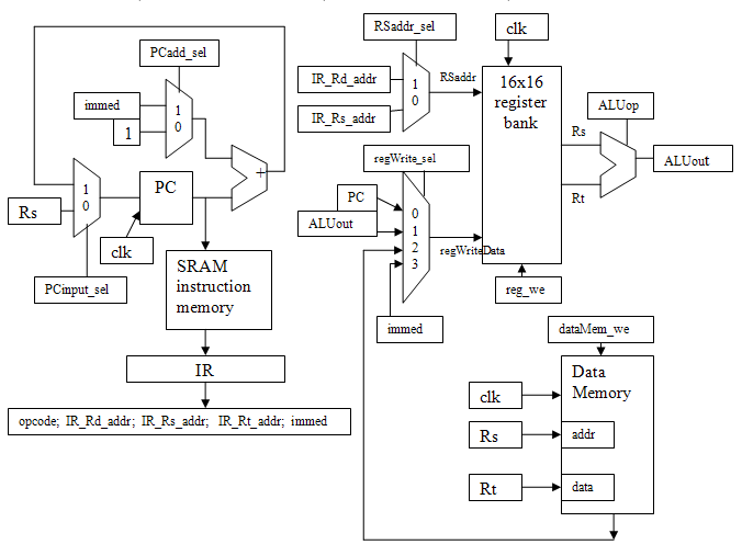
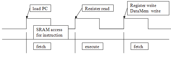
- Kraken 16-bit cpu
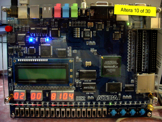
This example is a simple 16 instruction ISA cpu with LED and switch i/o. The implemented datapath and timing diagram are useful to understand the Verilog. There is a picture of the board displaying instruction address PC=02 which contains 16'h8104, which is the instruction LI r1,4 (load-immediate register1 with value 4). This cpu is mostly intended for me to teach myself Verilog in an Altera context.
Features include:
- Program storage in external, unclocked, static RAM. This has the advantage of not losing state every time the FPGA is reloaded. Programs are loaded the old-fashioned way, by toggling them in from switches during system reset.
- Programmer interface:
- SW16 forces reset when on. PC is set to zero on KEY3 clock
- HEX[3:0] 4 digit 7-seg display shows instructions if SW17=0 or data memory output if SW17=1
- SW[15:0] is used for input: instructions if SW17=0 or data bus if SW17=1
- HEX[7:6] 2 digit 7-seg display shows PC
- KEY3 is ~clock. This is used to run the cpu, to force a reset if SW16 is on, or to read data memory.
- KEY2 is write-enable in reset mode: instructions if SW17=0 or data if SW17=1
- KEY1 is inc/dec snoop address and KEY0 is snoop address clock. These keys can be used to manipulate the current address to instruction memory while adding/modifiing a program. They can also be used to read out a specific data address by setting the address, then toggling the clock (KEY3).
- HEX[5:4] 2 digit 7-seg display shows the snoop address set by KEY0/1: instruction memory if SW17=0 or data memory if SW17=1
- green LED 7 is Fetch/Execute with Fetch=on
- green LED 0 is data memory write_enable
- Registers and data-RAM specified according the Altera HDL style manual, so as to infer efficient M4K blocks during synthesis.
Two port, single read, single write RAM:
// data memory:
// single read and write
// taken from Altera HDL style manual page 6-17
// Synchronous RAM with Read-Through-Write Behavior
// and modified for 16 bit access
// of 256 words
module ram_infer (q, a, d, we, clk);
output  [15:0] q;
input [15:0] d;
input [7:0] a;
input we, clk;
reg [7:0] read_add;
reg [15:0] mem [255:0];
	always @ (posedge clk) begin
	if (we) mem[a] <= d;
	read_add <= a;
	end
	assign q = mem[read_add];
endmodule
Three port, dual-read, single write RAM (for registers)
// 16x16 register array
// with dual-read + write
// taken from Altera HDL style manual page 6-20
// modified for synchronous RAM with Read-Through-Write Behavior
// and modified for 16 bit access
// of 16 words
module dual_ram_infer (q, q2, write_address, read_address, read_address2, d, we, clk);
output  [15:0] q;
output  [15:0] q2;
input [15:0] d;
input [3:0] write_address;
input [3:0] read_address;
input [3:0] read_address2;
input we, clk;
reg [3:0] a1, a2;
reg [15:0] mem [15:0];
always @ (posedge clk) begin
	if (we) mem[write_address] <= d;
	a1 <= read_address;
	a2 <= read_address2;
end
assign q = mem[a1];
assign q2 = mem[a2];
endmodule
- Total resource use is about 1% of the DE2 FGPA (EP2C35F) logic elements and about 1% of onboard RAM. the cpu is mostly meant to be single-stepped to play with registers and memory.
Program:
   assembler        instruction memory
   LI r0, 1         8001 ;need to NOP first inst out of reset
   LI r0, 1         8001
   LI r1, 4         8104
   SUB r1 ,r1, r0   1110
   BNZ r1, -1       C1FF ;PC update timing implies that this jump is to the SUB
   JMP -3           E0Fd ;This jump is to the second LI
A short mpeg of this program executing. The finger entering the frame from the lower right is running the clock. The blinking green LED is illuminated during the FETCH state. The left-most 2 digit 7-seg display is showing the PC. The 4 digit 7-seg display is showing the instruction being fetched/executed. The program loops through the subtract 4 times, then jumps back, reloads the counters and down-counts again.
A possible variant is a simple cpu with i/o ports and a small ISA aimed at DSP. The implemented datapath and timing diagram are useful to understand the Verilog.
Features might include:
- Program storage in one M4k block. This design is meant for small applications.
- Data storage is 18-bit words in one M4k block. This design is meant for small applications.
- Multiply instruction compatable with the number system described on the DSP page.
References
JO Hamblen, TS Hall and MD Furman, Rapid protoyping of digital systems, Springer 2005
JO Hamblen, TS Hall and MD Furman, Rapid protoyping of digital systems: SOPC edition , Springer 2008
Nakano, K.; Ito, Y., Processor, Assembler, and Compiler Design Education Using an FPGA, Parallel and Distributed Systems, 2008. ICPADS '08. 14th IEEE International Conference on; 8-10 Dec. 2008 pages: 723 - 728
Nakano, K.; Kawakami, K.; Shigemoto, K.; Kamada, Y.; Ito, Y. A Tiny Processing System for Education and Small Embedded Systems on the FPGAs, Embedded and Ubiquitous Computing, 2008. EUC '08. IEEE/IFIP International Conference, Dec. 2008 pages: 472 - 479