Introduction
Digital Observer
We have built a scalable digital logic analyzer that is suitable to run on various hardware targets, allowing users without access to expensive lab instrumentation to perform useful debugging on various embedded platforms.
The What and the Why
As students in engineering we often find ourselves working with various communication protocols or in the need of a specific waveform. However, lab equipment which can output specific functions or analyze communications is often expensive. As such, our project presents the opportunity for students to be able to aquire such a tool for a fraction of the cost. By making use of an fpga we are able to decode communications in real-time while also allowing for software configurations from a HPS.
Overview
The project consists of two main pieces: a FPGA and a HPS. The FPGA is responsible for sampling data on a variable number of digital input channels. The FPGA performs decoding of SPI and I2C in hardware, and is also able to record the rising and falling edges of a signal to reconstruct the original waveform. The HPS is responsible for running a python based GUI which graphs the sampled data by reading it from the SRAM and ring buffers. The GUI also allows for software configuration of the analyzer blocks used in the fpga.
High Level Design
Project Rationale
The inspiration for this project came from the analog discovery product and our desire for a multi-tool which could analyze digital logic and output waveforms. In this day and age, accurate and reliable tools are often very expensive. As such, in classrooms and labs which need to have many setups, such expensive tools are not a viable option. Due to this, students are often left without a means of properly decoding logic which can cause frustration in the debugging process. As such, our group wanted to create a tool which would be cost effective for labs while also being useful for students. The solution we came up with was using SoCs/FPGAs to implement such a tool. In designing our project one of the decisions we made was to make our decoding blocks stampable. This means that we can chose how many blocks we want before hardware compile. This allows students to still use our project regardless of the SoC/FPGA system they are using, as they can customize the number of blocks to work with the amount of logic space their system has. For the GUI portion of this project we chose to x-forward our application. This allows students to run our application from their own devices without the need to install python or the various other packages used in the GUI.
Logical Structure
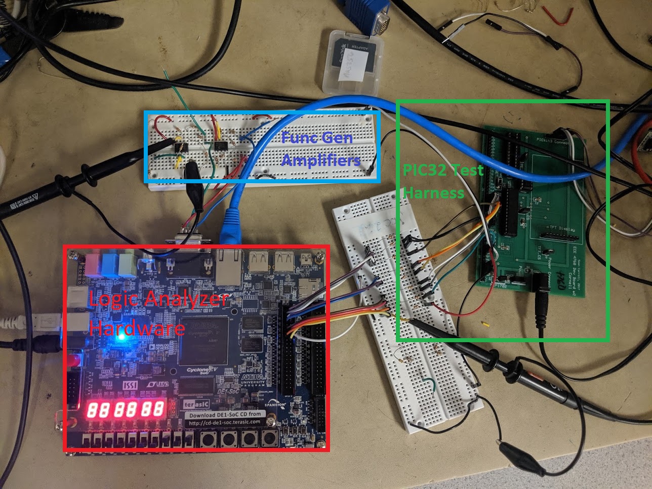
The project is split up into three main parts: the hardware logic analyzer / arbitrary function generator, the software GUI, and a PIC32 generating a series of test inputs. The hardware reads and decodes digital inputs as well as outputs arbitrary functions and is controlled by the GUI running in Python on the HPS, which can configure the hardware and show output to the user. In order to visualize useful inputs, a PIC32 generates PWM, I2C, and SPI inputs.
Hardware/Software Tradeoffs
There's various tradeoffs that we made in our design. The biggest, we think, is where the bus protocol decoding should happen. We chose to decode SPI and I2C in hardware because of the memory footprint savings that we could realize by encoding an SPI transaction as just the data. This did increase the design complexity, as it would have been easier to implement in software. Additionally, we lose some flexibility because now new bus protocol support requires hardware modification, which is a much larger endeavor than software changes.
Additionally, we chose to use Python as our GUI language, rather than C. While this did entail a lot more effort setting up packages (and even required us to switch operating systems entirely), it greatly increased the speed that we could iterate the GUI design. We also pay a performance cost with Python, since its an interpreted languge it will be significantly slower than C.
Program/Hardware Design
Program Details
GUI
To handle displaying of the decoded data we chose to implement a python based GUI which ran on the HPS. This decision was made since we used the DACs of the VGA output for our arbitrary function generator. As such, handling the GUI through the FPGA was not an option. Additionally, we chose to base our GUI on python's integrated tkinter library, since members of our group already had experience working with it. The GUI itself serves as the main method of observing the decoded data, and configuring the hardware crossbars and decoding blocks. The main window of our GUI can be seen in the image below.
Configs
One of the main functions of the GUI is the ability to reconfigure the hardware crossbars from software. This allows us to reassign pin inputs, decoder block functionality, and trigger conditions all without having to recompile the hardware itself. The image below shows an example of one of the decoder block configuration menus. As can be seen, the first line allows for the reconfiguring of the functionality of the decode block. This allows us to change which protocol the hardware is decoding on the fly. As such, the user is able to switch from decoding GPIO to SPI or I2C without needing a hardware recompile. Additionally, we can also set trigger conditions on the fly, allowing us to see the results of attempting to trigger on different events.
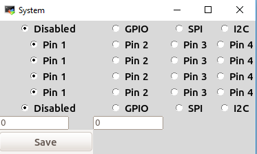
Actually configuring the fpga from software is broken up into two stages. The reason for doing so is so that more than one block can be configured at a time before sending the changes to the fpga. The first step is chosing the settings desired in the menu described above. Once the desired settings are chosen, selecting the save button sets the corresponding bits in the GUIs class variables. This is shown in the code below.
def save(decode_type, decoder_num, pin1, pin2, pin3, pin4, trig, trigCond, trigMask):
#We call .get() after each variable to obtain their integer forms
#This is because tkinter wdigets use tkinter variables which must be converted
gui.block_cfg[decoder_num] = decode_type.get()
print(gui.block_cfg[0])
if (decoder_num == 0):
gui.block1_pins[0] = pin1.get();
gui.block1_pins[1] = pin2.get();
gui.block1_pins[2] = pin3.get();
gui.block1_pins[3] = pin4.get();
gui.triggers [0] = trig.get();
gui.trig_cond = int(trigCond.get(),16);
gui.trig_mask = int(trigMask.get(),16);
#trig_cond and trig_mask are tk.StringVars and must be casted to int using base 16
A save function is tied to each decoder block menu and is unique for that block. Once the blocks have been configured accordingly, pressing the blue arrow button seen in the full GUI picture sends the configurations of each block to the fpga. The code for doing so is seen below. As the inputs to the set_pin_configs function is an array, we concatenate the pin configurations of each block into one array, which is then sent to the fpga.
def set_configs():
pins_config = []
pins_config.extend(gui.block1_pins)
pins_config.extend(gui.block2_pins)
pins_config.extend(gui.block3_pins)
pins_config.extend(gui.block4_pins)
h.set_pin_configs(pins_config)
h.set_trigger_config(gui.triggers[0], gui.triggers[1], gui.triggers[2], gui.triggers[3], gui.trig_mask, gui.trig_cond)
h.set_block_configs(gui.block_cfg[0], gui.block_cfg[1], gui.block_cfg[2], gui.block_cfg[3], gui.block_cfg[4])
Graphing
Arguably the most important feature of the GUI is the ability to graph the decoded data. To support this functionality, we make use of the matplotlib library for python. Each decoder block is given up to 4 subplots, one for each pin. In order to be able to update each plot as sampled data is read from the SRAM and ring buffers, we use the animate functionality of matplotlib. This allows us to call a plotting function for each series of subplots at a set time interval. To actually read in the data from hardware, we use our custom hardware/software interface. An example of how this is done is shown below. As can be seen we use the get_trigger_status() function of our interface to read in a 32 bit trigger status value. The MSB of this value tells us whether or not we have triggered. The following 2 bits describe which of the decoding blocks triggered, and finally the following 29 bits are the trigger address for the SRAM. If we have triggered than we read in data from the SRAM starting at the trigger address, and continuing for 500 samples. If we did not trigger, then we read in from address 0 to 500 from the SRAM.
trig_status = h.get_trigger_status()
trigger = bin(trig_status[0])
trigger_int = int(trigger,2)
check = int(trigger,2)
if(check != 0): #if it is 0, we did not trigger, and so the return value is 0
status = bitslice(trigger_int, 31, 31)
status_block = bitslice(trigger_int, 29, 30)
trig_addr = bitslice(trigger_int, 0, 28)
else:
status = 0
status_block = 0
trig_addr = 0
if (status and (status_block == 0)):
samples = h.read_samples(trig_addr, 500)
else:
samples = h.read_samples(0, 500)
Something to note as well is our ability to pause and start the plotting of sampled data. These actions are bound to the start and pause buttons seen in the overall GUI picture. Implementing this was fairly simple as we used a global pause variable, which we then wrapped our plotting functions in. Clicking the pause or start button would change this global value. Furthermore, through the use of the built-in matplotlib toolbars, users can zoom in on individual plots, save each plot for future analysis, and also adjust the settings of each plot without the need to re-launch the GUI.
Function Generation
The final aspect of our GUI is the ability to create abritrary waveforms by drawing them. While not necessarily useful in many situations, this allows us to confirm that our function generators are working properly. An example of this can be seen in the results section of our report. Pressing one of the three graphing buttons on the top right side of our GUI allows you to draw a waveform to be displyed through one of the three function generators. To draw waveforms we make use of the pygame library. This library allows us to draw a line whose coordinates are then returned when we finish drawing. These results are then used in our hardware/software interface to tell the function generator what to create. In the event that we draw a waveform with more than one y value for an x value, the larger y value is used for the function generation.
GUI Performance and X-Forwarding
The overall performance of the GUI is still in need of some work and there are several factors that play into this. The first factor would be the python libraries used. In order to graph our data we chose to make use of the matplotlib library. However, this is a fairly heavy library which adds a large workload to our procesor, especially when we need multiple plots going at a time. As the processor on-board is a simple micro controller, this often pushes the mcu to its limits. This can be seen in the fact that our processor usage jumps to nearly 100% when simply starting the GUI.
Another large factor in the performance issues of our GUI is x-forwarding. As mentioned earlier, we chose to use x-forwarding to allow users of our project to be able to run our GUI and hardware setup, without needing to install python or its packages onto their own machines. However, the downside of this appraoch is that x-forwading has a fairly large performance decrease due to the inherent design flaws of X11. X11 does not send the screen to the users machine, rather it sends display-instructions to a local X11 server, which the server then uses to re-create the screen on the users local machine. This must occur on each change/refresh of the display. As the local machine is not aware of what needs to be updated, and the remote server is also not aware of what the client needs, this results in large amounts of redundant data being sent. This is especially true in the case of animated graphs or images which our GUI makes uses of. In fact, in testing we were able to notice a signicant decrease in performance between when our graphs were updating, and when they were paused.
Moving forward we would likely look for an alternative to matplotlib. One of the potential solutions for increasing performance would be to output the results of the decoded communications as strings in a scrolling textbox. This would still allow the user to understand what messages are being sent over their communications lines, while eliminating the overhead of matplotlib. Most likely, we would present the user with the option to use either depending on their system specs.
Hardware Details
Analyzer Block Design
The analyzer block is a modular and configurable piece of hardware that performs all of the acquisition and decoding of the digital inputs. It has 4 inputs and is able to decode SPI and I2C, with a modular interface to allow more protocols to easily be supported. Additionally, it is able to record any rising and falling edges on a pin, so that all digital signals can be completely reconstructed. The block is reconfigurable at runtime, meaning that the crossbar connections, decode type, and trigger conditions can all be modified by the GUI without a hardware recompilation.
Decoding
This block supports decoding I2C or SPI, or simply recording each incoming rising and falling edge to completely reconstruct a given digital signal. Each decoder receives inputs from the input crossbar, which is capable of remapping any of the four external facing inputs to the pins of the decoder. The decoders need to know which pin is the clock, data, or any other important signals to a specific protocol. The input crossbar allows the user to plug in the signals any way that they like, and using the software interface, they can let the hardware know how they connected their signals, rather than forcing the user to use specific pins for specific signals.
Decoding SPI
The SPI decoder is relatively straightforward. A transaction begins when the CS line is pulled low. With the CS low, the decoder will shift in a new value from MOSI and MISO every rising edge of SCK. When CS is brought high, if the decoder senses that an entire transaction has happened, the SPI values will be sent to the analyzer block. This means that the decoder will throw away transactions that do not send the full 8 bits, to avoid misidentifying malformed transactions. An example in ModelSim is shown below.
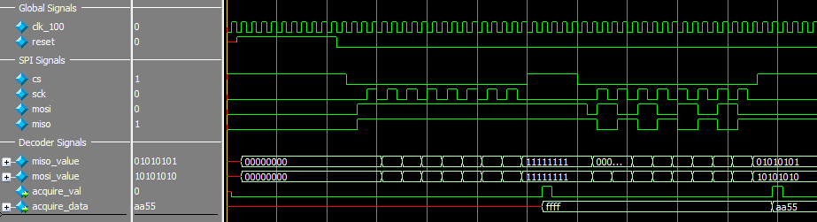
The above snapshot of ModelSim shows how the decoder behaves given two different SPI transactions. The first transaction shows 0xFF on both the MOSI and MISO lines. We can see that the internal “miso_value” and “mosi_value” signals update with each rising edge of SCK. When we reach the end of the transaction, both of these signals represent the values sent across the bus. When CS is pulled high, the two miso and mosi values are packed into a single result called “acquire_data,” and the “acquire_val” signal is asserted to let the analyzer block know that it should grab this decoder’s data. SImilarly, another SPI transaction immediately follows the first, this time sending 0xAA and 0x55 on the MOSI and MISO lines. Just like the previous transaction, the values of “mosi_value” and “miso_value” are updated as bits arrive, and eventually the output is latched and the valid bit asserted.
Decoding I2C
Decoding I2C was slightly less straightforward than SPI. An I2C transaction consists of four main parts: a START condition, 8 bits of data, an ACK/NACK, potentially a STOP condition. This decoder keeps track of whether the start is a repeated start or not, the 8 bit data, whether there was a NACK or an ACK, and whether a STOP was asserted.
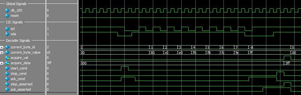
The above waveforms from ModelSim show an example I2C sending 0xFF with a start and an ACK. We can see the “current_byte_id” increase from 0 to 7 as the rising edges of SCL clock new values on the bus. The byte value is slowly constructed throughout the transaction, resulting in a 0xFF value returned to the analyzer block. From the signals toward the button of the picture, we can see the various points at which the START, ACK, and STOP conditions are asserted.
Triggering
The trigger unit can be configured to trigger on a number of different events. It can trigger on any rising or falling edge of any of the inputs, or a masked transaction value from one of the decoders. For example, this means it is possible to trigger on the following conditions:
- On any rising edge
- On the falling edge of pin 1 OR the rising edge of pins 2 and 3
- When 0x42 is send over SPI
- When the first four bits of an I2C transaction are 1
Analyzer Clump Design
Our design allows for a number of analyzer blocks to be stamped out. This modular design was implemented to allow our design to be run on a variety of hardware platforms, with the number of decoder channels able to scale with the available hardware on the target device. We call the grouping of analyzer blocks a “clump,” and the figure below attempts to illustrate the various components of this module.
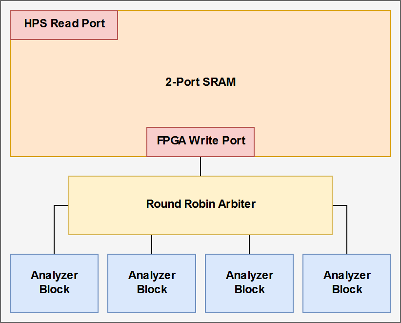
The variable number of analyzer blocks are all connected to a Round Robin Arbiter. Each of the analyzer blocks is attempting to write samples to the shared SRAM. This arbiter was sourced from the vc library provided by the ECE 4750 and ECE 5745 courses at Cornell. The arbiter takes in a bit vector of requests, which are entities requesting access to a shared resource, which is the shared SRAM in this case. The blocks only assert their request when they have data waiting in their internal buffers to write. The round robin arbiter will accept requests in a round robin fashion, attempting to be as fair as possible while ensuring that only one analyzer block is granted permission to write to the SRAM on a given cycle.
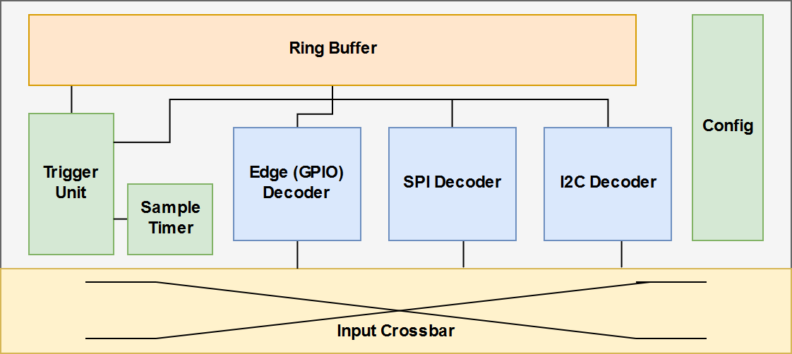
Latency Insensitive Communication
Since our analyzer blocks will be producing results at unknowable times (since the data directly corresponds to outside inputs) we felt that a latency insensitive interface that can tolerate quick bursts of data would be the most appropriate. All of the analyzer blocks share a common SRAM where they write their sample data to. This is to ensure maximum memory utilization (partitioning into multiple SRAMs could potentially be very wasteful) and reduce software complexity. The diagram below shows how we structured our interfaces.
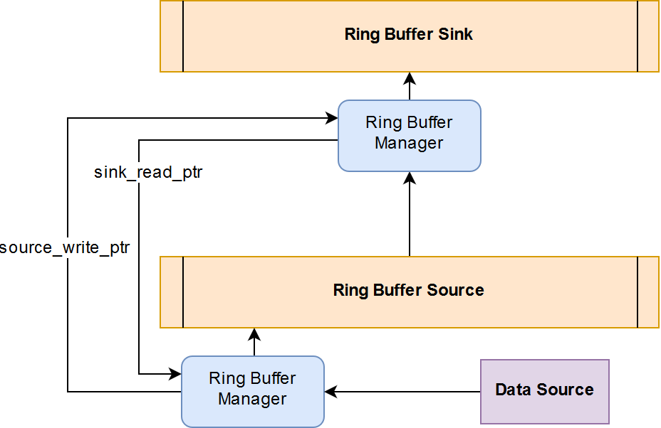
For each ring buffer, a corresponding “Ring Buffer Manager” would keep track of its relevant metadata. Each ring buffer has a read pointer and a write pointer, where the read pointer describes where in the buffer the reader is, and the write pointer describes where the writer is. If the write pointer is behind the read pointer, then there is space to write. If the write pointer is at the read pointer, the buffer is full and we cannot write. There is similar logic for the read pointer. If the read pointer is in front of the write pointer, then we can read, but if the read pointer is just behind the read pointer, then the buffer is empty and we cannot read. The ring buffer managers take the role of disguising the ring buffer as an infinite string of memory, for easy use by both reader and writer logic.
Function Generator Design
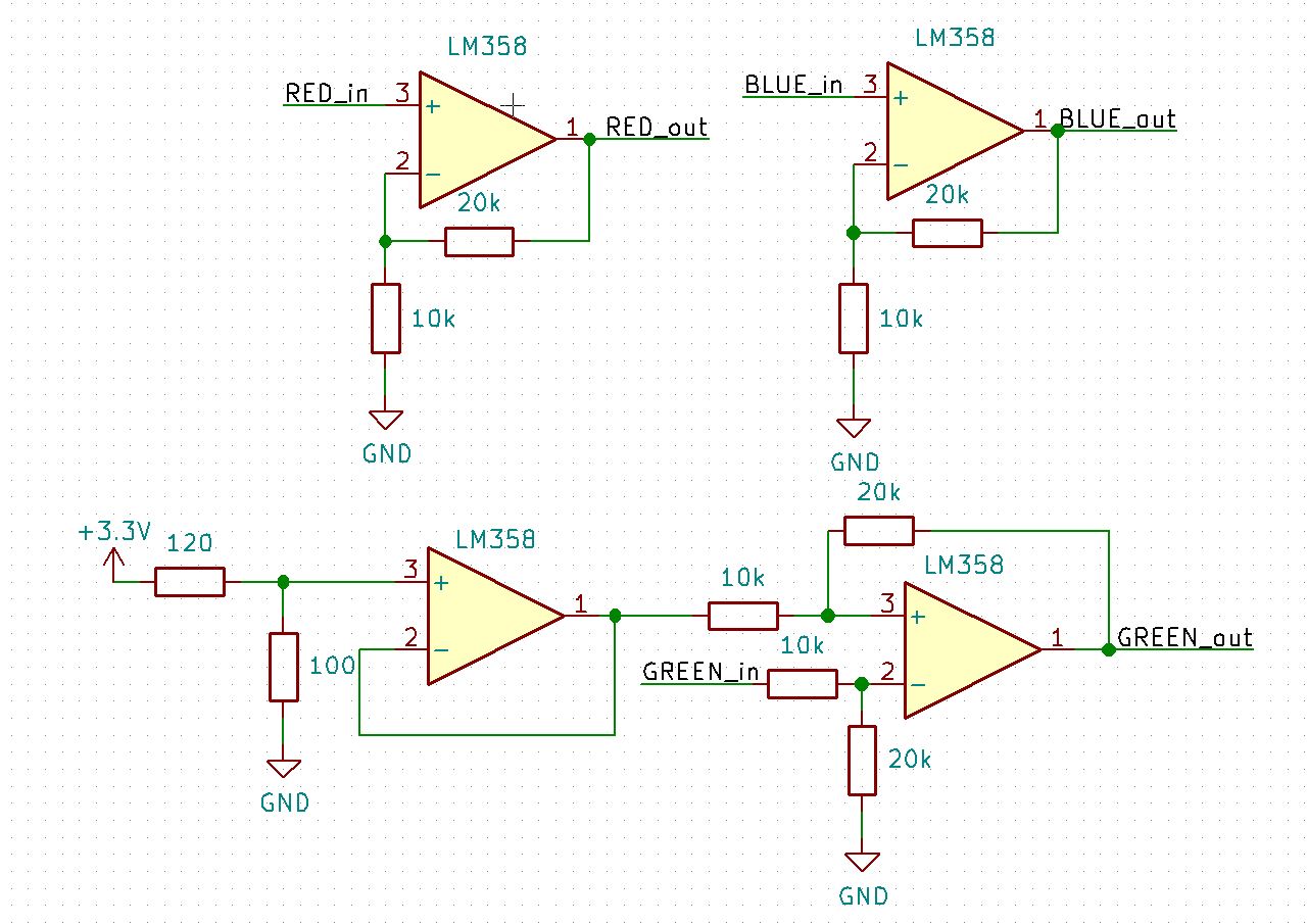
The function generator implementation uses the onboard 3-channel DAC that is meant to drive the R, G, and B components of a VGA signal. Instead, we use each as an 8-bit DAC channel to generate arbitrary functions. Each channel has an SRAM that contains the points to output. The SRAM is controlled by software and each function generator cycle, a new sample is read out from the SRAM and outputted on the DAC. The function generator also has a prescaler that can be used to adjust the rate at which samples are read from the SRAM. This is so the user is not locked in to the sample rate of the FPGA clock, and they can choose an arbitrary prescaler value to slow the clock down. The SRAM is writeable from software and easily controllable by the GUI.
Realtime testing with PIC32
In order to test the decoding capabilities of our logic analyzer, we decided it would be best to use a PIC32 to generate realworld waveforms. Thanks to Prof. Bruce, we were able to use the PIC32 Boards and PIC microstick from ECE4760 to make this part of the project relatively straight forward. To test correct functionality, we required waveforms for various GPIO signals, SPI, and I2C. The PIC outputted 4 GPIO signals, all of different duty cycles and periods. For SPI, the PIC acted as the master and transmitted values from 0-255 repeatedly and slowed it. For the I2C protocol, we ended up bitbanging specific values, as we ran into some problems using the I2C peripherals on the PIC32.
We use the following code to shift the PIC32 into slave mode:
// Open SPI Channel 2 as master (@500 kHz) 8 bit mode
SpiChnOpen(spiChn, SPI_OPEN_ON | SPI_OPEN_MODE8 | SPI_OPEN_MSTEN | SPI_OPEN_CKE_REV , spiClkDiv);
// SDO2 (MOSI) is in PPS output group 2, could be connected to RB5 which is pin 14
PPSOutput(2, RPB5, SDO2);
PPSInput(3, SDI2, RPB13); // RBP13 --> SDI2
PPSInput(3, SS2, RPA3); // RPA3 --> Chip select
The interrupt service routine code for SPI:
// CS low to start transaction
mPORTBClearBits(BIT_4); // start transaction
// test for ready
while (TxBufFullSPI2());
// write to spi2
WriteSPI2(count++); //send values 0-255
// test for done
while (SPI2STATbits.SPIBUSY); // wait for end of transaction
// CS high to end transaction
mPORTBSetBits(BIT_4);
Results
Logic Analyzer Sampling
In our final design, we created a 16-channel digital logic analyzer (more channels can easily be added on). Each sample holds one of the following: the rising/falling edges of each of the 4 inputs, an SPI transaction, a I2C transaction. Samples are timestamped and labeled with the time they were sampled at and the block that sampled it. Our 46-bit timestamp gives no issues with overflow, and we can track the time of a sample very accurately. The total sample bitwidth is 64-bits in this implementation. However, hardware decoding saves a lot of data. For example, if we are sampling SPI at 20 MHz using four continuous sampling channels, we produce data at a rate of (20*4) 100 Mbps. However, if we decode the SPI transactions in hardware and we assume that the average SPI channel is at most producing transactions 50% of the time, then we can fully encode the SPI channel while only needing a throughput of 1.25 Mbps.
We have been able to record 4 GPIO channels, 1 SPI channel, and 1 I2C, where each GPIO channel was toggling at about 500 kHz, and the SPI and I2C channels were transmitting as fast as a PIC32 could transmit (@ 20Mhz and 100kHz, respectively). For screenshots of this result, see the video and the GUI section.
Arbitrary Function Generator
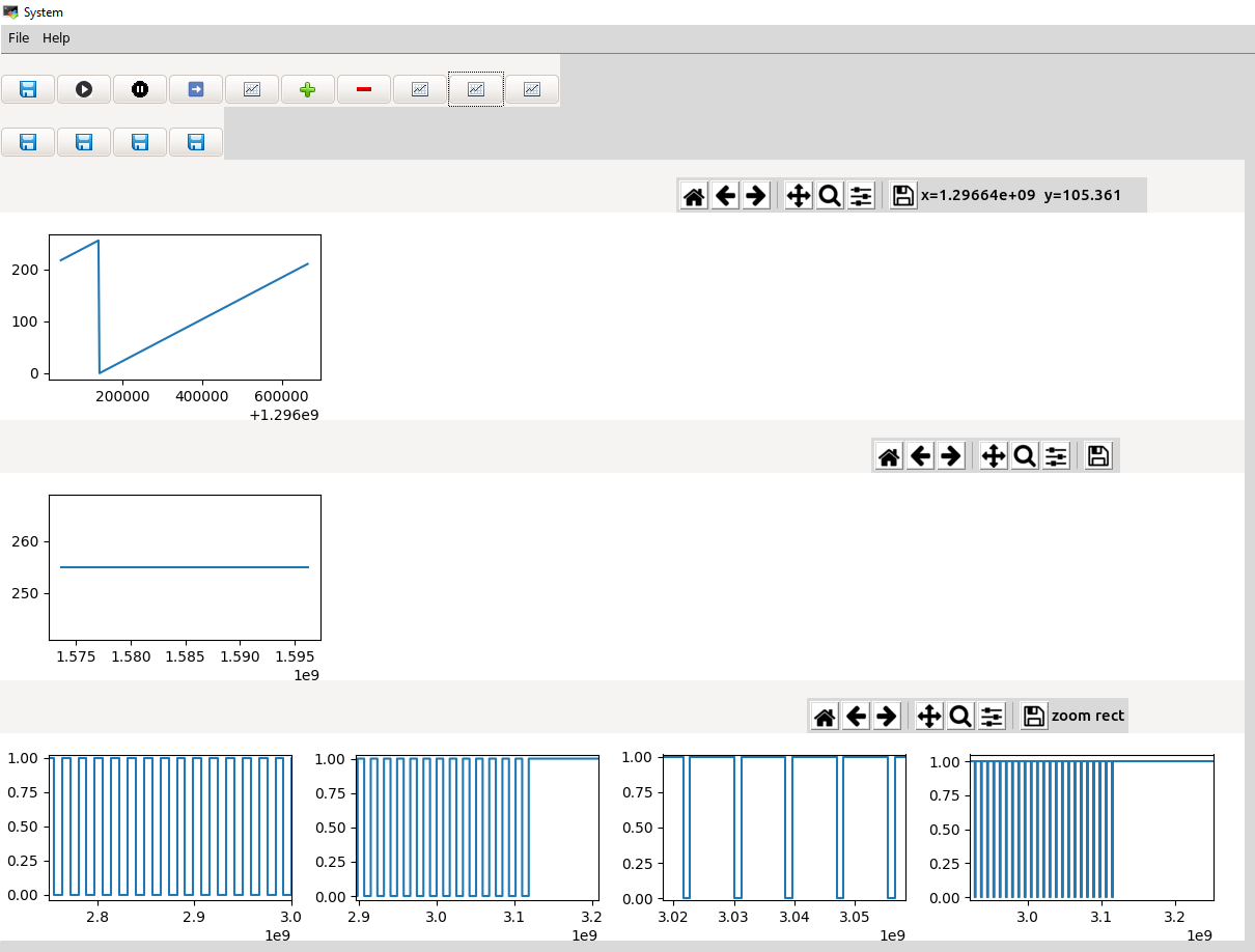
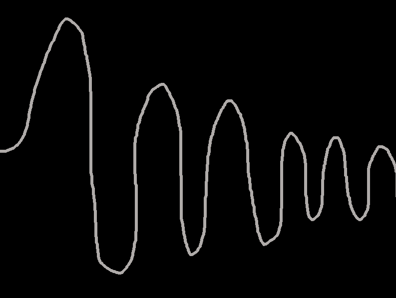
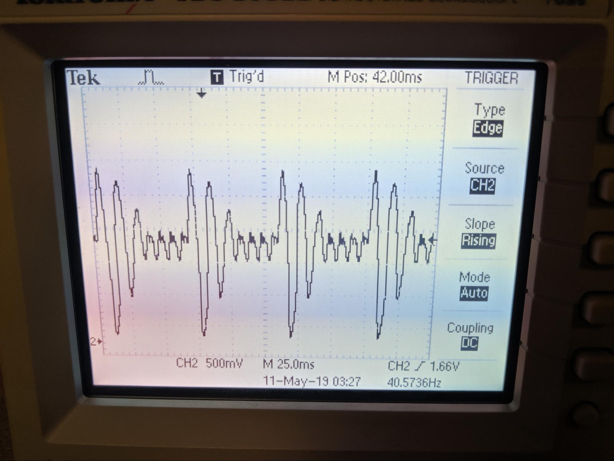
Our design also supports the inclusion of a 3-channel arbitrary function generator. There are some preset patterns such as triangle waves and square waves, but we also included the ability to draw a waveform and have it recreated on the DAC output. This is shown below. The drawn waveform is at the top and the corresponding output is shown below it.
Conclusions
Expectation versus Reality
We are quite pleased with how the project turned out. While we were able to get a fully functioning GUI running on the HPS, we had to make some compromises because X-Forwarding is slow, especially because of the relatively weak compute power of the embedded HPS cores. We couldn't use many of the graphics libraries we wanted to and the reponse time of the GUI was less than we'd hoped for. But overall we are very happy with the project and feel that it fully meets the original goals that we initially set out to achieve.
Legal and Intellectual Property Considerations
To produce this project we used various FPGA IP provided by Altera through their Quartus IDE. We do not plan to distribute or sell this software or hardware. All other code is our own unless stated otherwise in a file header or in this report. We have used some library code released in ECE 4750 and have cited our uses of this code. We omit this from the public release however, as we have not obtained explicit permission to release it to the public.
Appendix
The group approves this report for inclusion on the course website. The group approves the video for inclusion on the course youtube channel.
The commented Verilog code for our project can be found here.
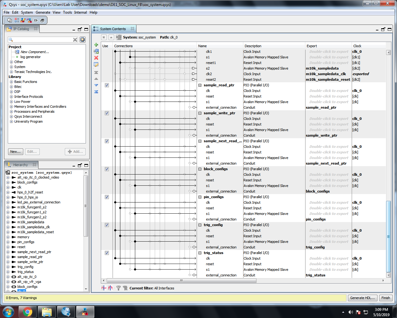
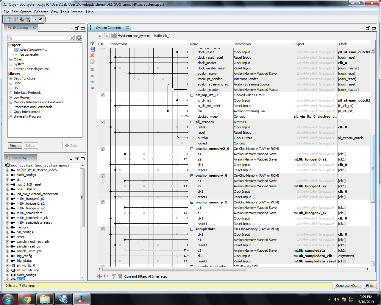
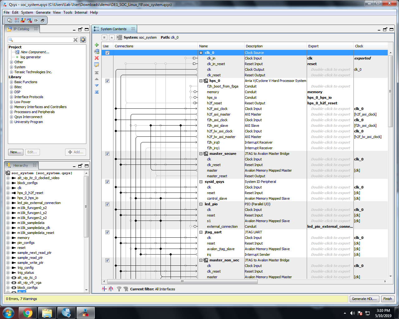
Screenshots of our QSys Configuration can be found here, here, and here.
The commented PIC32 C code for our project can be found here.
Verilog Code
The commented Verilog code for our project can be found here.
QSys Screenshots
Screenshots of our QSys Configuration can be found here, here, and here.
C Code
The commented PIC32 C code for our project can be found here.
Task Distribution
While the vast majority of the project was a combined effort, Nick mostly focused on the hardware implementation, Julia focused on the PIC32 test bench, and Anthony focused on the Python GUI. This breakdown allowed us to work in parallel and be much more productive than we otherwise could.
Acknowledgements
We are extremely grateful to Bruce Land for helping us through various problems throughout our design. The knowledge and intuition that he was able to share with us saved us a lot of time debugging and allowed us to quickly realize our ideas. The great ecosystem that he has built on both his ECE 4760 and ECE 5760 websites makes development much more streamlined.