Abstract:
This project implements a DDR RAM controller at the RTL level for the
Altera Cyclone II FPGA on a DE2 development board. A PCB board was also
designed and fabricated to provide an interface between the FPGA and the
memory chip. DDR RAM is a widely used memory standard designed to provide
storage and retrieval of large amounts of data at very high clock frequencies.
The main distinction between this type of memory and other standards is that
data is read and written on both rising and falling edges of the input clock. The
motivation behind choosing this project was my desire to complement my
classroom experience in designing digital systems on the FPGA with a real world
application. This standard is used in many different digital systems, including
high-performance graphics cards and modern personal computer systems. The
challenge in this project is to develop a state machine capable of handling
inputs at high clock frequencies while still maintaining an acceptable level of
performance. The controller hardware was implemented using Verilog and the
PCB board was designed using the ExpressPCB design software.
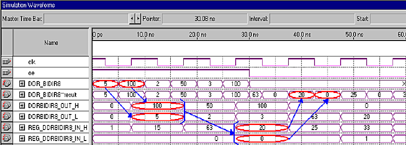
Simulation and verification was done in a Linux operating system
environment. iVerilog was used to synthesize the code and run a simulation, and
GTKWave was used to observe the output waveform and perform debugging.
Micron provided a Verilog model of the DDR RAM, which was used inside a
testbench along with DDR control module. The model provided feedback as to
whether the DDR chip was receiving the proper input signals. A design flaw in the
Terasic DE2 board prevented me from implementing my top file on the
Cylone II FPGA.
Full Report (PDF)
Source code (PDF)
Source code (ZIP)
In order to run the simulation script, the user will need to have Linux and iverilog installed.