Abstract:
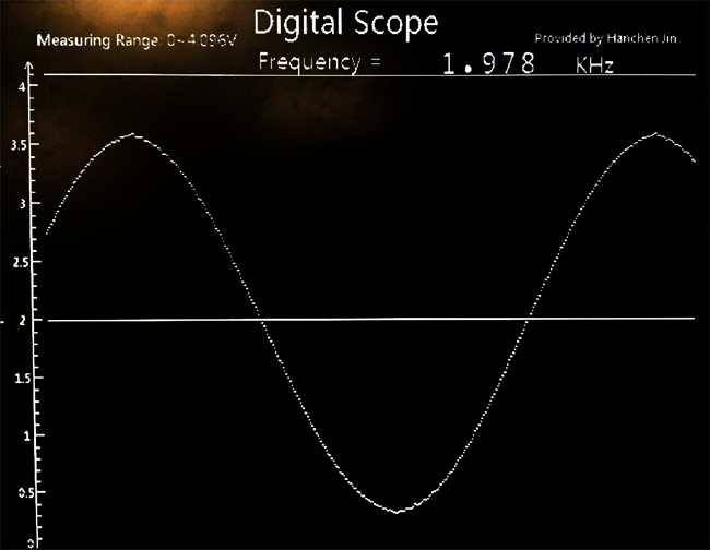
The objective of this project is to implement a digital oscilloscope based on Alter DE1-SoC board. Since DE1-SoC has a low-noise, eight-channel CMOS 12-bit analog-to-digital converter (LTC2308) with a conversion throughput (Sample Rate) up to 500Ksps, it can be an appropriate hardware platform for implementing a digital oscilloscope. Also a 15-pin D-SUB connector is available on this DE1-SoC board which is driven by the ADV7123—triple 10-bit high-speed video DAC (transforms signals from digital to analog). This DAC can support the SXGA standard (1280x1024) with signals transmitted under a speed up to 100MHz. For implementing the stable displaying, VGA mode (640x480) within a 25MHz pixel clock is chose as the display configuration for this design. The ADC values are stored into two register arrays—one for stable displaying, one for buffering ADC data for next frame; then these data are operated by FPGA logic and used to draw waveform on monitor through VGA port. Since FPGA logic is able to do parallel floating operations effectively, it can calculate the frequency of the waveform and also update the display on the monitor quickly. So this design builds a digital scope including the functions like measuring and storing voltage for DC or AC value, adjusting trigger value, adjusting horizontal position of the waveform, calculating the frequency, run/stop, reseting the whole system and selecting ADC value input channels by the combination of switches and buttons. It is mainly comprised of ADC measuring module, data storage and calculation module and VGA displaying module. All of these functions are implemented in FPGA logic.
Report (pdf)
Poster (pdf)