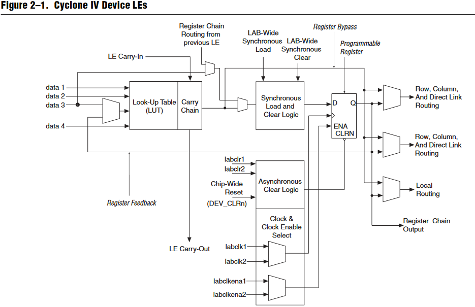
logic element modes normal and arithmetic.
22k LE is enough to build a few 32-bit processors on one chip.
Statments in Verilog: set up the LUT, set the MUXs, and route the output to other LEs and to memory
An FPGA is an integrated circuit which can be programmed after manufacture to become the hardware that you describe. The DE0-nano that you are using can be a 32-bit cpu, a VGA-controller, or camera controller. Or all three. The process for specifying the hardware depends on a high level hardware language called Verilog. You might use a FPGA when you need highly parallel computing or huge i/o bandwidth.
You are going to need a FPGA because of the high-speed timing demands and bandwidth required to generate a VGA image,
while handling a communications connection to an Arduino.
-- You will get a maze description from the Arduino via SPI channel that you build.
-- Construct an image in FPGA memory from the maze description
-- Build a VGA controller that generates sync and copies FPGA image memory to the 8-bit VGA DAC at 60 images/sec
-- DAC has 3 bits of red, 3 bits of green, and 2 bits of blue.
320x240x8-bits x 60 fps = 614400 bits x 60 = 36.8 Mbits/sec
-- Generates a tune when the maze is completely mapped.
FPGA structure
Your FPGA has:
--Logic elements 22,320
--Memory blocks
594kbits, mostly as M9k blocks
--Dedicated, very fast, hardware, multipliers
66 18x18 multipliers
--A variety of clock sources
Logic element
logic element modes normal and arithmetic.
22k LE is enough to build a few 32-bit processors on one chip.
Statments in Verilog: set up the LUT, set the MUXs, and route the output to other LEs and to memory
Logic Array Blocks (LAB) are groups of LE organized for fast communication.
Each LAB consists of the following features:
--
16 LEs: convenient for 32 bit arithmetic with fast LAB carry chains and two arithmetic bits per LE
--
LE carry chains and Register chains
Memory
Using LE as memory:
-- Fast to set up
-- Asynchronous access and global clear possible.
This allows you to do operations you cannot do on M9k blocks.
--
inefficient use of FPGA resource (relative to M9k blocks).
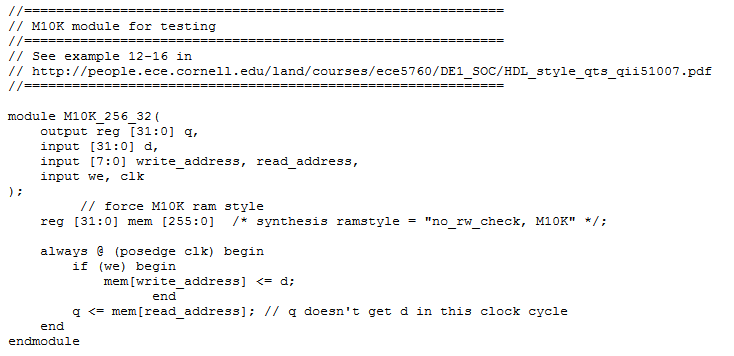
M9k block memory:
--
Single port RAM, Dual port RAM, FIFO, Shift register, ROM.
-- Synchronous access only, must use clocked registers.
-- Arranged as 1, 2, 4, 8, 9, 16, 18, 32, 36 bit words for total of 9k bits each.
-- Verilog can specify memories spanning multiple M9k blocks (see below)
Multipliers
-- 9x9, 18x18, or chained in Verilog for more bits
-- Fast, single cycle operation up to several 100 MHz for 18x18.
Your DE0-nano board also has
-- 32MB SDRAM
-- IF you intend to use this you MUST first learn to use the Qsys bus tool!
-- 8 LEDS
-- Two pushbuttons
-- ADI ADXL345, 3-axis accelerometer
-- ADC
-- 50MHz clock oscillator, which can be modified in the FPGA using a PLL for different frequencies
(e.g. VGA clock rate 25.175 MHz)
Using Verilog to describe hardware
The abundance and variety of hardware on the FPGA demands design automation tools.
You will be using Verilog organize your design at the register-transfer level RTL.
You will specify registers, wires, memories, arithmetic and all other logic in Verilog.
Verilog looks a lot like C-language, but it is fundamentally different.
(More Verilog detail from ece5760)
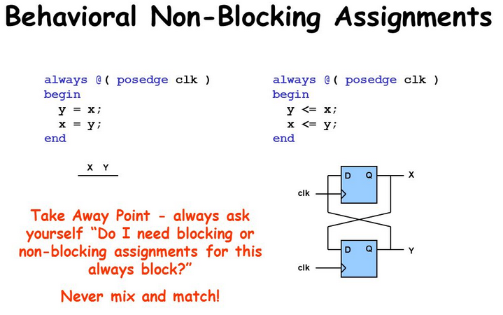
Verilog Style
-- Nonblocking Assignments in Verilog Synthesis, Coding Styles That Kill!
-- Avoid inferred latches
Verilog simulation/testbench
-- Local ModelSim example
-- Testbench Primer
Verilog Examples
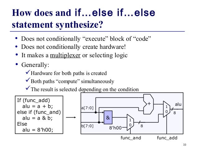
Making a multiplexer (combinatorial --notice blocking assign)
-- combinatorial block
always@(a or b or sel)
   if (sel == 1’b1)
      c = a;
   else
      c = b;
-- Ternary operator
wire c = sel ? a : b;
Making a state machine (clocked -- notice non-blocking assign)
-- direct digital synthesis (see also the full code)
module DDS (clock, reset, increment, phase, sine_out);
input clock, reset;
input [31:0] increment ;
input [7:0]  phase;
output wire signed [15:0] sine_out;
reg [31:0]	accumulator;

always@(posedge clock) begin
	if (reset) accumulator <= 0;
	// increment phase accumulator
	else accumulator <= accumulator + increment  ;
end

// link the accumulator to the sine lookup table
sync_rom sineTable(clock, accumulator[31:24], sine_out);
-- and the ROM table
module sync_rom (clock, address, sine);
input clock;
input [7:0] address;
output [15:0] sine;
reg signed [15:0] sine;
always@(posedge clock)
begin
    case(address)
    		8'h00: sine = 16'h0000 ;
		8'h01: sine = 16'h0192 ;
		8'h02: sine = 16'h0323 ;
		8'h03: sine = 16'h04b5 ;
		8'h04: sine = 16'h0645 ;
            ...
                8'hfe: sine = 16'hfcdd ;
		8'hff: sine = 16'hfe6e ;
	endcase
end
endmodule
Making dual port memory (clocked), e.g. VGA frame buffer.
This module infers M9k memory in Quartus Prime, when using Cyclone4.
RAM-style determination and page 12-15 in HDL style guide
module single_clk_ram(
    output reg [7:0] q,
    input [7:0] d,
    input [6:0] write_address, read_address,
    input we, clk
);
    reg [7:0] mem [127:0];
    always @ (posedge clk) begin
        if (we)
            mem[write_address] <= d;
        q <= mem[read_address]; // q doesn't get d in this clock cycle
    end
endmodule
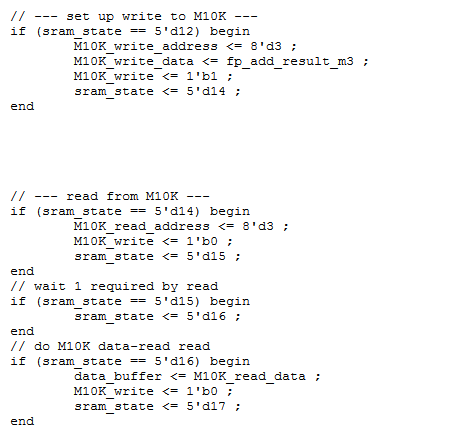
Defining RAM, instantiating it, state machine to drive it.
(from the last example on 5760 memory page)
Define the memory module.
Instantiate the memory
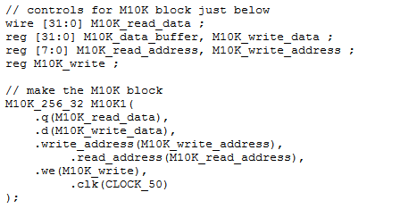
Read/write memory (note 1 wait state on read)
Advanced synthesis cookbook (Intel)