ECE 4760 Final Project
NFC Transmitter and Receiver
Lingnan Liu (ll656) and Jilong Wu (jw859)
Introduction High Level
Design Hardware
Design Software
Design Testing Strategy and Results Conclusion Appendices
Introduction
Our project is building one set of NFC module including a NFC transmitter and a NFC receiver both using ATmega1284p microcontroller. We will be using coupled coils to transmit message modulated by a high frequency carrier, whose frequency is the standard frequency for Near Field Communication (NFC) – 13.56MHz (Wikipedia, 2013).
In our project, we build a local oscillator which generates the accurate NFC carrier by using the crystal oscillator circuit. To set up the near field wireless transmission, we build two coupled coils as antennas to transmit and receive the message, which is the application of resonant inductive coupling. These two coils are tuned to resonate at the frequency of 13.56MHz. We use one ATmega1284p microcontroller to generate the message and modulate it with the carrier from our local oscillator. The modulated high-frequency signal will be transmitted through the coupled coils to the receiver including a transistor amplifier, a hysteresis comparator and another ATmega1284p microcontroller which processes the received signal and displays it through serial port.
As opposed to many colleagues who make complicated design with very dedicated application, we choose to dive into the working procedure of the wireless module and build it from scratch. The goal of our project is not a very detailed application, but a basic method of transmitting message through wireless channel which can be utilized by a large amount of applications. Through this project, we hope to make ourselves clearer about the working procedure of transmitting message at radio frequency and improve our practical skills.
High Level Design
Background
Near Field Communication (NFC) is a new technology that has emerged in the past decade. It is a set of standards for smartphones and similar devices to establish radio communication with each other by touching them together or bringing them into close proximity, usually no more than a few inches. This idea was originally used by radio-frequency identification, or RFID. RFID allows a reader to send radio waves to a passive electronic tag for identification, authentication and tracking. NFC, inherited from the working scheme of RFID, is only capable for a short range communicating and thus inherent secure data exchange can be applied. Many individuals and companies have seen the great potential of this new technology and thus many applications have been developed. For example, a company named Log-IC has used NFC tags to keep track of thermometer readings of temperature sensitive goods. Google also developed Google Wallet using mobile NFC. Currently, integration of NFC technology into mobile phones has been proved a practical solution. This creates a potentially huge market for NFC applications because nowadays almost everyone has a cellphone. All those novel NFC products are interesting and its promising future motivates us to figure out the pros and cons of this technology. Thus, we decided to build our own NFC module which can be used for extensive applications in the future.
Overview
In our design, we intended to use LC tank to work as antenna. Since the standard working frequency for NFC transmitter is 13.56MHz, the LC product is required to be very small. It turns out that the self-tuned inductor (coil) has the resonant frequency of 13.56MHz. We build our own 13.56MHz oscillator to work as the carrier frequency. The digital message from ATmega1284p is modulated by the carrier frequency and then transmitted through the wireless channel. Because of the loss during the transmission, the voltage of the received signal is not high enough to trigger comparator. To solve this problem, we build a unity-gain amplifier whose output is low voltage for input 1 with high frequency signal and high voltage for input zero. Then we use inverting comparator with hysteresis whose output signal is 5V for digital 1 and 0V for digital 0. Output from the amplifier is inverted after the comparator and hence the original digital message is restored. Then this restored digital signal is processed in ATmega1284 and the message is displayed through serial port.
Logical Structure
1. Hardware
The hardware of this project is composed of two main parts, transmitter and receiver. Transmitter block includes user interface (ATmega1284p), local oscillator (13.56MHz carrier generator) and antenna (LC Tank). Receiver block includes antenna, demodulation and ADC Circuit (unity gain amplifier and hysteresis comparator with inverting-input) and signal processing (ATmega1284p).
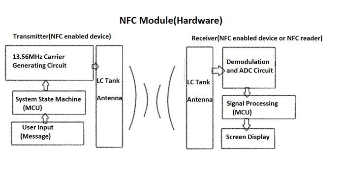
Figure 1
Components of NFC Module (Hardware)
2. Software
We will be using USART1 on
ATmega1284p microcontroller to transmit and receive messages. To transmit a
message, we first put it into a transmit buffer which will be sent through TX1
(PD3) one character at a time. For reception, hardware USART will automatically
read bits from RX1 (PD2) and put it into UDR1 (USART Data Register). All we
need to do is just read from this register and put it into a receive buffer
which be further processed later.
3. Hardware and Software Tradeoff
The first tradeoff we have is the processing of the received signal. Since our transmission is achieved at a high frequency (13.56MHz), the loss during the transmission is relatively high. The voltage of received signal is quite low (around 300mV). Converting this low amplitude, high frequency signal into digital signal is really tricky. If the demodulation and ADC tasks are done by the microcontroller, more complex software processing method is required. This rapidly increases the computation burden of the microprocessor. However, if we use some hardware to share tasks of signal processing, the workload of the microprocessor will be reduced. Also, the signal is easily converted to desired digital signal by using our circuit implantation. Details about the implementation are described in the latter section.
4. Related Standards
In
our project, the transmission frequency we use is 13.56MHz. It is within the
band of 13.110 and 14.110 MHz. Thus, it is regulated by FCC 15.209 and FCC
15.229.
(a) The field strength of any emissions within the band 13.553-13.567 MHz shall not exceed 15,848 microvolts/meter at 30 meters.
(b) Within the bands 13.410-13.553 MHz and 13.567-13.710 MHz, the field strength of any emissions shall not exceed 334 microvolts/meter at 30 meters.
(c) Within the bands 13.110-13.410 MHz and 13.710-14.010 MHz the field strength of any emissions shall not exceed 106 microvolts/meter at 30 meters.
(d) The field strength of any emissions appearing outside of the 13.110-14.010 MHz band shall not exceed the general radiated emission limits in § 15.209.
(e) The frequency tolerance of the carrier signal shall be maintained within ±0.01% of the operating frequency over a temperature variation of −20 degrees to 50 degrees C at normal supply voltage, and for a variation in the primary supply voltage from 85% to 115% of the rated supply voltage at a temperature of 20 degrees C. For battery operated equipment, the equipment tests shall be performed using a new battery.
(f) In the case of radio frequency powered tags designed to operate with a device authorized under this section, the tag may be approved with the device or be considered as a separate device subject to its own authorization. Powered tags approved with a device under a single application shall be labeled with the same identification number as the device.
Table 1 FCC Regulations
|
Frequency(MHz) |
Field Strength(microvolts/meter) |
Measurement distance(meters) |
|
0.009-0.490 |
2400/F/(kHz) |
300 |
|
0.490-1.705 |
24000/F/(kHz) |
30 |
|
1.707-30 |
30 |
30 |
Since our project is just building a
prototype of NFC Module not for commercial use, the following standards are not
required here (http://www.waazaa.org/download/), but for further application
development, these standards must be taken into consideration.
Near Field
Communication has a standard working frequency of 13.56MHz and for 13.56MHz air
interface communication, ISO/IEC 18000-3
is required.
NFC standards cover communications protocols and data exchange formats, and are based on existing radio-frequency identification (RFID) standards including ISO/IEC 14443 and FeliCa. The standards include ISO/IEC 18092 and those defined by the NFC Forum, which was founded in 2004 by Nokia, Philips Semiconductors and Sony.
5. Existing Patent and Copyright
For our oscillator design, we used the design idea from the
website of Home of the Z80 CPU. We modified the design to work at 13.56MHz for
our project. Also, we modified the comparator design from Cornell University
ECE4760 Lab4.We changed it into an inverting hysteresis comparator with
different reference voltage.
Hardware Design
Coil Antenna
The antenna is built using two coils. The wireless transmission
between these two blocks is done using resonant inductive coupling. A coil with oscillating current will
generate an oscillating magnetic field. Other coil nearby will be driven by the
oscillating magnetic field and hence signal will be transmitted.
Since our transmission is done at a high frequency, the parasitic capacitance takes a huge effect. A real coil can be approximately modeled as shown in Figure 2. Cp is the parasitic capacitance and R is resistance under DC voltage.
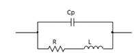
Figure 2 LC Tank Circuit
The resonant frequency given by this RLC model is 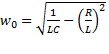 . While, it is very hard to control the value
of the parasitic capacitance (resistance can be ignored for long distance coil).
The method we used here is measuring the self-resonant frequency of the coil
and then adjust the size of the coil accordingly. After picking the coil with a
certain inductance, we measure its self-resonant frequency. If this frequency
is lower than 13.56MHz, we need to scale down the size of the coil. The
inductance of a coil is given by the equation
. While, it is very hard to control the value
of the parasitic capacitance (resistance can be ignored for long distance coil).
The method we used here is measuring the self-resonant frequency of the coil
and then adjust the size of the coil accordingly. After picking the coil with a
certain inductance, we measure its self-resonant frequency. If this frequency
is lower than 13.56MHz, we need to scale down the size of the coil. The
inductance of a coil is given by the equation ![]() where D = coil diameter in inches, N = Number of turns, l = coil length in
inches. So the inductance of the coil becomes smaller if we reduce the number
of turns of the coil. Also, reducing the turns of the coil will decrease the
parasitic capacitance as well since the parasitic capacitance is from the
individual wire turn of the coil. If the picked coil has a self-resonant
frequency higher than 13.56MHz, a capacitance (
where D = coil diameter in inches, N = Number of turns, l = coil length in
inches. So the inductance of the coil becomes smaller if we reduce the number
of turns of the coil. Also, reducing the turns of the coil will decrease the
parasitic capacitance as well since the parasitic capacitance is from the
individual wire turn of the coil. If the picked coil has a self-resonant
frequency higher than 13.56MHz, a capacitance (![]() )
can be added in parallel with the coil to increase the resonant frequency. We
assume the resonant frequency after adding
)
can be added in parallel with the coil to increase the resonant frequency. We
assume the resonant frequency after adding ![]() is
is ![]() and
and ![]() for
for ![]() .
By using this two sets of data we can find the value of L and Cp.(If you want
to make it more precise, you can measure a third set of data
.
By using this two sets of data we can find the value of L and Cp.(If you want
to make it more precise, you can measure a third set of data ![]() to find value of R). For our own experience, after
reducing the coil size for three times, we happened to get a coil with a approximate
self-resonant frequency of 13.56MHz. One thing to mention here consider the
transmitting efficiency will be affected by inductance. The maximum achievable
efficiency is
to find value of R). For our own experience, after
reducing the coil size for three times, we happened to get a coil with a approximate
self-resonant frequency of 13.56MHz. One thing to mention here consider the
transmitting efficiency will be affected by inductance. The maximum achievable
efficiency is  ,
where
,
where ![]() ,
,  ,
, ![]() ,
, ![]() , and
, and ![]() are the Q facor of the transmitter and receiver coils.
After some math, we can obtain
are the Q facor of the transmitter and receiver coils.
After some math, we can obtain ![]() approximately, If
we deduce the inductance by cutting turns, which will make Q smaller and hence
the efficiency will become lower.
approximately, If
we deduce the inductance by cutting turns, which will make Q smaller and hence
the efficiency will become lower.
Carrier Frequency Generation
Before a digital message being transmitted through wireless
channel, it must be modulated to a higher frequency which is more suitable for
wireless transmitting. ATmega1284 is running at a frequency 16MHz and its
actual frequency upper bound is a lot lower. We cannot use MCU to generate a
13.56MHz signal so an oscillator is required. Our oscillator is a modified
design from Home of the Z80 CPU, the schematic is shown in the red block in Figure 3. Basic idea to
build an oscillator is an amplifier with a feedback network. In order for an
oscillator to operate, two conditions must be satisfied: a. the loop power gain
must be equal to unity; b. the loop phase shit must be equal to 0, 2pi, 4pi,
etc. The exact frequency at which an oscillator will operate is dependent on
the loop phase angle shifts within the oscillator circuit. The most common
method to provide a stable net phase shift is to use a quartz crystal unit in
the feedback loop. Figure 3 shows a
depcition of the rectacne vs. frequency of a quartz crystal unit. As we can see
from the plot, a quartz will have two frequencies of zero phase fs and fa. fs is referred as the series resonant
frequeny and the higher one, fa, is
reffered as the parallel frequency. At the seris resonant point, the resistnace
is minimal and the current flow is maximal. At the prallel reonant point, the
resistance is maximal and the current flow is minimal. Therefore, the parallel
resonant frequency should never be used as the controlling frequency of an
oscillator circuit. Thus, we choose a series reonsant osicllator cirucit design
as shown in Figure 4. The two resitors are used to bias the invertor and the
invertor will operate at its linear region. The resistor also provides a
negative feedback to the invertor. The 100nF capacitor is used to block DC
voltage. The 22pF capacitor is used to bias the crystal at high frequecny. We
choose these values so that the series resonant oscialltor will operate at the
natural frequency of the crystal, which is 13.56MHz.
Figure 3
Reactance vs. Frequency Plot of a Quartz Crystal Unit
Digital
Modulation (On-off Keying)
We
used On-off keying (OOK) for our digital modulation. It is the simplest form of
amplitude-shift keying modulation (ASK) that represents digital data as the
presence or absence of a carrier wave (Wikipedia). The presence of a carrier
for a specific duration represents a binary one while its absence for the same
duration represents a binary zero. OOK is easier to implement and more
spectrally efficient than other modulation scheme. Thus, we pick this method
for our digital modulation.
The
signal out of OOK modulation can be expressed in the form:
where
![]() is the modulated signal,
is the modulated signal, ![]() is the digital signal to be modulated and
is the digital signal to be modulated and ![]() is the carrier.
is the carrier.
For
circuit implementation, as shown in Figure 3, message is converted into digital
high/low voltage signal by the microcontroller. The digital signal and carrier
frequency (13.56MHz) are combined together. It will be a high frequency signal
for binary 1 while absence of this signal for binary zero.
Figure 4
Transmitter Schematic
Demodulation and Analog to Digital Conversion
The receiver schematic is shown in Figure 5. As discussed in the previous session, to couple the coil to work at a frequency of 13.56MHz, the inductance of the coil is quite small. This leads to low transmission efficiency. The amplitude of the received signal is only around 300mV. This signal is way too small and thus demodulated by an envelope detector seems not practical. We need to amplify this signal first.
However, another problem appeared. The received modulated signal has a high frequency with certain amplitude while almost zero amplitude when not sending message. After the amplifier, the high frequency will be amplified while the zero amplitude input will turned into high voltage (which is 5V for our project). If we continue to use a high pass filter, the amplitude will be abated again and still envelop detector will not work.
After some observation, we realized that since the purpose
of this demodulation and ADC block is to restore the original digital signal
from the received analog signal, we can process the signal after amplifier
directly. If we design a unity-gain amplifier, the zero input will become high
voltage after being inverted by the amplifier while the high-frequency, low
amplitude part will have similar amplitude which is a low voltage output. In
this way, output after amplifier will be high voltage for input low and low
voltage for input high. The design of the unity-gain NPN amplifier
is shown in in the orange block
in Figure 5.
After signal is processed by the unity-gain amplifier, we
use an inverting hysteresis comparator to convert it back to the signal which
can be used directly as logic 1 and logic 0. Output from the amplifier will be
fed into the inverting comparator. When input voltage is above ![]() ,
the comparator will output voltage low, which is 0V for our project. The output
will not change until input voltage is blow
,
the comparator will output voltage low, which is 0V for our project. The output
will not change until input voltage is blow ![]() .
Then the comparator will output voltage low.
.
Then the comparator will output voltage low.
We set ![]() = 3.5 V and
= 3.5 V and ![]() = 0.5V. After some math using
equations:
= 0.5V. After some math using
equations: ![]() ,
we find
,
we find ![]() and
and![]() .
The schematic of this inverting hysteresis comparator is shown in red block in Figure 4. The comparator
converted analog input into digital output and this output will then be
processed and analyzed by the microcontroller.
.
The schematic of this inverting hysteresis comparator is shown in red block in Figure 4. The comparator
converted analog input into digital output and this output will then be
processed and analyzed by the microcontroller.
Figure 5 Receiver Schematic
Software Design
The responsibility of the driver
software of our NFC module is divided into two parts. For the transmission
part, the driver needs to accept the string that user want to transfer, form
the data packet and send it through USART. For the reception part, the driver
needs to read from the USART, write into receiver buffer and return the right
string that user want to receive. We design our NFC communication library
according to the standard C criteria, with NFCPack.h containing the declaration
of functions and variables and NFCPack.c including their implementations.
Data Packet Format
Our data packet begins with a start
token ‘#’, which reminds the receiver of the presence of valid data. Following
parts are the transmitter id, data string (payload) and two checksums. One last
character is the end token ‘%’, which indicates the end of valid data. The
checksums are calculated only corresponding to the payload and are sent together
with the data. It will serve as the reference checksum at the receiver side
where the checksum will be calculated again and compared with the reference to
eliminate possible transmission error.
This data packet format is inspired
by the packet format we have been using through the infrared communication lab.
We think this format can protect the data from being interfered and retain its
integrity as most as possible. The disadvantage of this data packet is that the
start token and end token cannot be used in the payload as this will break the
data packet and mislead the receiver. However, this problem can be resolve
simply by using different unprintable characters as the start token and end
token.
Timer 0 Interrupt and USART1
We use USART1 on ATmega1284p
microcontroller as the transmitter port and receiver port. Baud rate setting is
in NFCPack.h. For now, we can sustain 19200 baud with no transmission error,
which is a very high baud rate compared to the infrared communication system.
The Timer/Counter 0 is set to CTC
mode and serves as a 1ms time base. Every 1 millisecond, the interrupt service
routine will send and receive a character through USART1.
Important Library Functions and Macros
1. NFC_UART_BAUD:
Baud rate setting macro
By redefining this macro, the baud
rate of NFC communication can be changed. Now the highest baud rate we sustain
is 19200 baud.
2. nfc_send_packet: Transmit a
string
Its prototype is
void nfc_send_packet(char tx_id, char
data[]);
This function is used to send the
string stored in data[]. A transmitter id must be provided as the first
argument of this function. This function will be blocked until every character
in the string is sent so DON’T use it in timer interrupt service routine.
3. nfc_rec_packet: Receive a
string
Its prototype is char
nfc_rec_packet(char tx_id, char data[]);
This function is used to receive a
data string and store it into data[]. A transmitter id must be provided as the
first argument of this function. This function will use the transmitter id as
reference and only receive the data packet that has the particular transmitter
id. A number will be returned indicating the status of the transmission: 0
means good data, 1 means buffer overrun, 2 means no data (time out), 3 means
bad transmitter id, 4 means bad checksum.
Testing Strategy and
Results
Hardware Test
As shown above, the main challenging
point in our design is the hardware part. Thus, we also pursue our most test effort
in hardware side. Following the incremental design and unit
test strategy, the hardware testing
for this project is divided into two phases:
Phase 1: we
individually test the functionality of every block
We first provided DC voltage for
oscillator and checked the frequency of the output signal at the static state. We
adjust the size of the capacitor to make it oscillate at a frequency around 13.56MHz, which serves as the carrier frequency. Then we modulate that carrier frequency with the
message to be transmitted, which is compared with the
original digital message to check if the modulated signal is what we want. The carrier waveform is shown in Figure 5 and the
modulated signal is shown in Figure 7.
To test the functionality of the coil
antenna, we use a function generator to generate a
13.56MHz signal which is feed to the
transmitter end and check the received signal on the receiver end to see if
signal can be transmitted and large
enough. This test should pass easily since we have already used this
method to test when we adjust the size of the coil. The received signal at the receiver end is shown in
Figure 8.
Phase 2: we
connect all the blocks together and test the whole system
We pursue the whole system test only
after the unit test of every individual module have passed, eliminating the
chance that one glitch in one block ruins the whole system. We connect the
blocks together to form the whole NFC transmitter/receiver and measure the
waveform of every relevant point in circuit to test the functionality of the
whole system. In this phase, we measure the waveform of the amplified received
signal and the signal after comparator, shown in Figure 9 and 10.
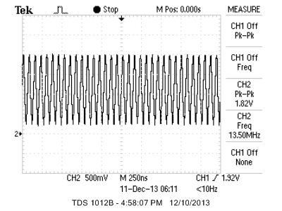
Figure 6 Carrier Wave around 13.56MHz
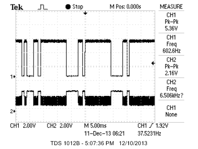
Figure 7 Modulated Signal
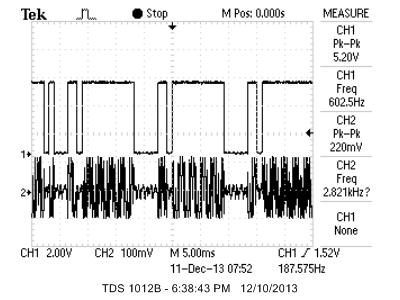
Figure 8 Received Signal
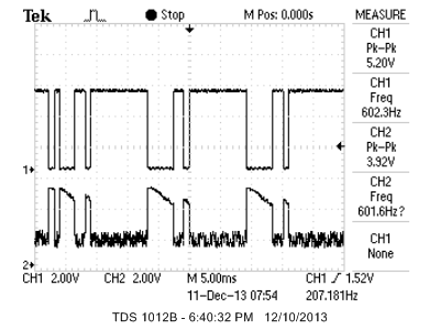
Figure 9 Amplified Signal
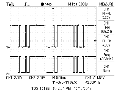
Figure 10 Restored Signal (After Comparator)
Note that the upper signal in Figure 7,
8, 9 and 10 is the original message from the transmitter. Comparing it with the
signal we process, we can see that our circuit does work as intended:
transmitting the message and receiving it with no distortion.
Software Test
The test of our software (aka. the
driver to implement the data package format and the NFC communication library)
is also very important. We write a simple C program named NFCTest.c to test the
functionality of our NFC communication library.
NFCTest.c utilizes Tiny Real Time
multitasking kernel to implement the transmitter task and the receiver task.
These two tasks act like state machines whose state transition diagrams are
shown in Figure 11 and 12.
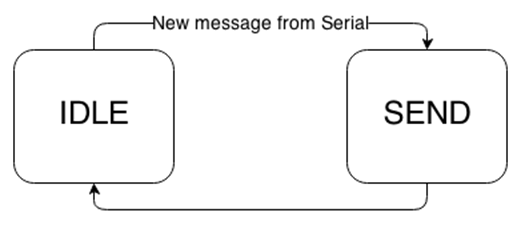
Figure 11 State Transition of Transmitter Task
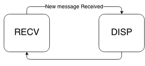
Figure 12 State Transition of Receiver Task
Transmitter task will wait in IDLE
state until new message from serial port input by us comes in. Then it will
turn to SEND state and transmit the new message using our library function:
nfc_send_packet(). Once the transmitting is finished, transmitter task will
return to IDLE state waiting for the next message.
Receiver task tries to receive the
packet in RECV state. Once the packet is valid, it turns to DISP state to
display the payload through the serial port. Then it returns to RECV state
waiting for the new data packet.
Through the test, we find that our
NFC communication library functions normally as intended.
Results
The picture of the NFC transmitter
and receiver we built are shown in Figure 13 and 14.
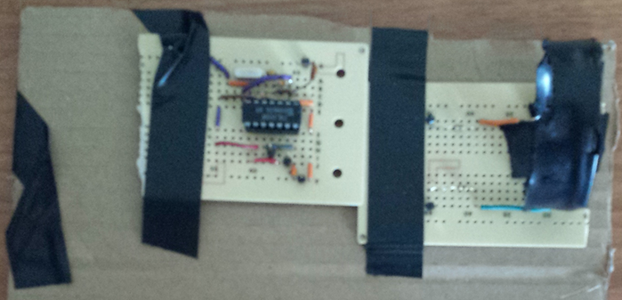
Figure 13 Transmitter Hardware (without MCU)
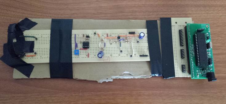
Figure 14
Receiver Hardware (with MCU)
The performance metrics of our design is shown in Table 2.
Table 2 Comparison between Our Design and Other Similar Technology
|
|
Our Design |
Common NFC Reader |
|
|
Working Frequency |
13.56MHz |
13.56MHz |
|
|
Response Time |
0.1s |
<0.5s |
|
|
Baud Rate |
19200 |
Very high |
|
|
Range |
2cm |
<10cm |
|
|
Cost |
$51* |
~$50 |
|
Note that the cost for our project is around $51. This cost is calculated using ATmega1284p. However, if this module can be scaled down to PC board and embedded into mobile cellphone, the cost for MCU will be excluded.
As shown in the performance metrics, our design has similar performance as general NFC reader in market nowadays. However, what we have done is based on lab facilities from class and it is a rough design. More improvements can be performed and better performance (smaller size, faster response time, lower cost, etc) is achievable.
For further improvements, we will first scale down the device size of the system. Printed PCB boards will be designed and manufactured. Also, we will use TR package for ATmega1284p. This package will have smaller size and lower cost.
For applications, many ideas can be applied using this NFC module:
-Home Auto Switch
We can use NFC module as switches to control Wi-Fi, Bluetooth and turn up or down the volume of stereo system at home. Whenever we left home, we can just put our phone close to a NFC tag and turn off the Wi-Fi or Bluetooth in a convenient way.
-Business Card in Wallet
NFC Module can be used to read information from a NFC tag in a wallet. This tag can store any information like name and job. This tag will work as an electronic business card. As long as a NFC reader is close to the tag, the information can be read and analyzed.
-Locking Door
NFC Module can built to lock or unlock our door. The microcontroller built inside the NFC module can used to control mechanical lock system. As more and more smartphone will have a NFC module in it, you can just wave your cellphone towards the door and you can lock or unlock the door within a very short time.
-Business Advertisement
We can print out NFC tags to advertise our own business. When someone sees the NFC tag, they can use their cellphone to scan it and it will show the location of our business on google map. It is much faster than QR code. The response time for the NFC reader in market is less than 0.5s.
Conclusion
Summary
In the final project, we manage to
build our own NFC module consisting of NFC transmitter and receiver. The module
is able to work properly at the frequency of 13.56MHz with 0.01% error rate and
a working range of 2cm. The cost is $51, within the budget. What we will do
differently next time is to develop more useful applications for this project
based the module. Several interesting ideas have been discussed in the Results
section. Also, if we do it differently next time, we will use a high gain amplifier
and an envelope detector to demodulate the signal instead of one unity-gain amplifier.
We will compare the performance of these two system in terms of response time,
maximum baud rate, error rate, etc.
As discussed in Results, our NFC module has similar performance metric as
common NFC Reader in market. Also, it follows FCC regulations as discussed in Legal
Considerations. If this module is developed for
other applications including commercial uses, many other standards from RFID regulations
and NFC forum must be taken into consideration.
Intellectual Property Considerations
The
code we used for our design is originally written by our team for ATmega1284p. For
hardware design, we used the oscillator design idea from the website of
Home of the Z80 CPU. We modified the design to work at 13.56MHz for our
project. Also, we modified the comparator design from Cornell University
ECE4760 Lab4.We changed it to an inverting hysteresis comparator with different
reference voltage.
Ethical Considerations
Our project strictly follows IEEE
Code of Ethics. As discussed in the previous part, our design is a prototype
for NFC applications. These applications include smart lock, temperature tag,
etc. People will benefit a lot from these applications of NFC. These
applications will keep the safety, health and welfare of the public. Meanwhile,
it will keep any harm that may cause danger to them. We tested our design by
measuring signals from different blocks using oscilloscope. We summarized our
results based on the real data from measurement. We don’t accept any form of
briberies. In the background and results
section, we discussed many applications that can be used based on our NFC
module and as mentioned in Conclusion, we will transform this design into print board
which has smaller size and more stable performance. We also have talked about
the limitations of our design. We are open to any form of criticism and
suggestions regardless of race, religion, gender, disability, age or national
origin. All the design is done carefully and thoughtfully to avoid injuring
others or infringe upon other people’s reputation, property, etc. Both our team
members assist each other to solve technical problems and also learn to follow
IEEE Code of Ethics.
Here we would like give special
thanks to our instructor Bruce Land and TAs who gave us tremendous instructions
to improve our design not only in class, but also during lab work. We also
would like to thank website Home of the Z80 CPU which gives us the idea
for our basic design.
Legal
Considerations
In our project, the transmission
frequency we use is 13.56MHz which is regulated by FCC 15.209 and FCC 15.229.
We fulfilled all the requirements.
The
field strength of any emissions within the band 13.553-13.567 MHz shall not
exceed 15,848 microvolts/meter at 30 meters. Since our transmission has a very short range of 2cm, the field
strength is very small at 30 meters. Thus, this requirement will be satisfied
for the NFC module we built.
Within
the bands 13.410-13.553 MHz and 13.567-13.710 MHz, the field strength of any
emissions shall not exceed 334 microvolts/meter at 30 meters. This is not
required for operating frequency of 13.56MHz.
Within
the bands 13.110-13.410 MHz and 13.710-14.010 MHz the field strength of any
emissions shall not exceed 106 microvolts/meter at 30 meters. This is not
required for operating frequency of 13.56MHz.
The
field strength of any emissions appearing outside of the 13.110-14.010 MHz band
shall not exceed the general radiated emission limits in §
15.209. This is not required for operating frequency of 13.56MHz.
The
frequency tolerance of the carrier signal shall be maintained within ±0.01% of
the operating frequency over a temperature variation of −20 degrees to 50
degrees C at normal supply voltage, and for a variation in the primary supply
voltage from 85% to 115% of the rated supply voltage at a temperature of 20
degrees C. For a temperature of 20 degree C, we changed the supply voltage
within the range of 85% to 115% of the rated voltage, the frequency changes
within 13.48MHz to 13.60MHz which is within ±0.01% of 13.56MHz. Also, due to
limitations of testing equipment, we are not able to test it over a temperature
variation of -20 degrees to 50 degrees C at normal supply voltage. But for
further development of this product, the temperature test will be conducted in
high priority.
In
the case of radio frequency powered tags designed to operate with a device
authorized under this section, the tag may be approved with the device or be
considered as a separate device subject to its own authorization. Powered tags
approved with a device under a single application shall be labeled with the
same identification number as the device. Since we are not building radio frequency
powered tags in our project, we don’t need to worry about this regulation.
Table 3 FCC Regulations (FCC 15.209)
|
Frequency(MHz) |
Field Strength(microvolts/meter) |
Measurement distance(meters) |
|
0.009-0.490 |
2400/F/(kHz) |
300 |
|
0.490-1.705 |
24000/F/(kHz) |
30 |
|
1.707-30 |
30 |
30 |
As discussed in the first part, since
our project is just building a prototype of NFC Module and not for commercial
use, standards ISO/IEC 1800, 0-3, ISO/IEC 18092, ISO/IEC 14443 and FeliCa and those defined by the NFC Forum are not required here, but for further application development,
these standards must be taken into consideration.
Appendix A Relevant Source Code
1. NFCPack.h: The declaration
of the NFC communication library;
2. NFCPack.c: The
implementation of the NFC communication library;
3. NFCTest.c: The test
benchmark of the NFC communication library.
Appendix B Hardware
Schematic
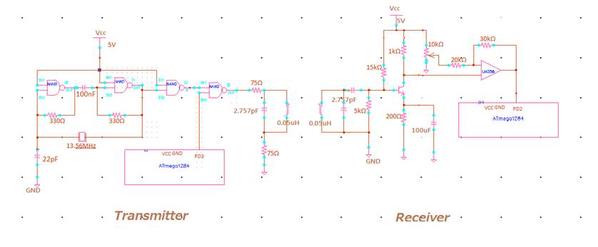
Figure 15 NFC Module
Appendix C
Cost Details
Table 4 Cost Details
|
Part |
Description |
Quantity |
Unite Price |
Total Price |
Supplier |
|
ATMega1284p |
MCU |
2 |
5 |
10 |
Bruce Land |
|
DIP Socket |
For MCU, NAND Gates, Op-amp |
3 |
0.5 |
1.5 |
Bruce Land |
|
Pin Header |
Connections within each board and between
different blocks |
74 |
0.05 |
3.7 |
Bruce Land |
|
NPN 2N3904 |
Unity-gain Amplifier |
1 |
0.2 |
0.2 |
Bruce Land |
|
Custom PC board |
MCU board |
2 |
4 |
8 |
Bruce Land |
|
RS232 connector for custom PC board |
Serial Connector for PC board |
2 |
1 |
2 |
Bruce Land |
|
LM358 |
Comparator |
1 |
0.5 |
0.5 |
Bruce Land |
|
MAX4233 for custom PC board |
Serial Connector for PC board |
2 |
7 |
14 |
Bruce Land |
|
Solder Board |
For transmitter and receiver board |
4 |
2.5 |
10 |
Bruce Land |
|
13.56MHz crystal |
For oscillator design |
1 |
0.56 |
0.56 |
Digikey |
|
74LS00N |
NAND gates for oscillator |
1 |
0.67 |
0.67 |
Bruce Land |
|
Total Cost |
|
|
|
51.13 |
|
Appendix D
Task Distribution
Table 5 Task Distribution
|
Lingnan Liu |
Jilong Wu |
|
Code and Software Test |
Hardware Design (70%) |
|
Website (50%) |
Hardware Test |
|
Hardware Design (30%) |
Website (50%) |
|
Soldering |
Soldering |
Appendix E References
Datasheets:
References:
Oscillator Design Consideration
15 Creative and Useful Ways to Use NFC Tags with Your
Smartphone http://trendblog.net/creative-and-useful-ways-to-use-nfc-tags-with-your-smartphone/