cuDVF: Affordable Shaft Vibration Analysis
Anthony McNicoll and Jonathan Wu
We brought an old piece of purpose-built mechanical engineering equipment into the modern age by implementing its functionality on a microcontroller and streamlining its user interface.
Introduction
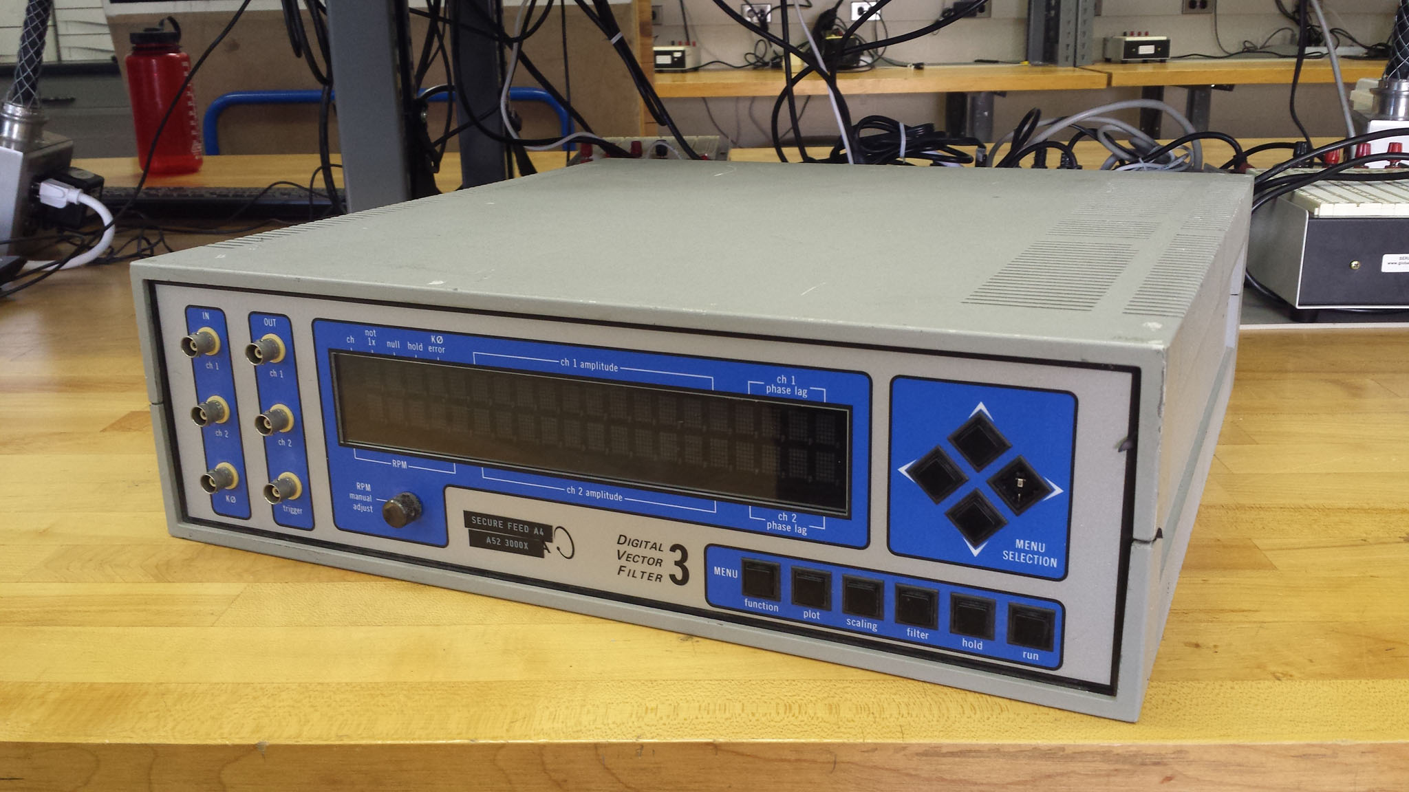
Our objective is to reproduce the function of the Bentley-Nevada DVF3:
This piece of lab equipment dates from 1988 and is used in Cornell’s mechanical engineering department (as well as around the world) as a training tool to measure shaft displacement, and consequently, shaft vibrations. Its core functionality is to take in sine-like proximitor signals (which could be biased anywhere from -9 to +6 volts, with amplitude up to about 7 volts) and measure the phase, frequency, and amplitude of the shaft displacement.
During the course of an instructional lab, students also use many of the device’s extra features:
- Measurement and subtraction of a “null vector” corresponding to the shaft’s low-frequency displacement due to bends/surface finish rather than vibrations
- Plotting information over GPIB, e.g. for making Bode plots
- “Peak hold” of frequency and phase at the maximum amplitude, and amplitude itself
- Generation of an output signal with no DC offset and with null vector compensation
These boxes are no longer made new. Despite being 25 years old, calibrated units go for $1500 on auction sites. We constructed the cuDVF, which achieves comparable performance for less than a tenth of the price.
High-Level Design
Because we aimed to develop a device to replace the DVF3 in an instructional lab setting, we focused on implementing only the features used during the course of an instructional lab, and streamlining common procedures. The more formal originating requirements of interest are then:
- Measure RPM from a "keyphasor" known to be a square wave from -15V to -10V
- Measure the pk-pk amplitude of two sine-like proximeter signals in the -15V to 0V range
- Measure the phase lag of two sine-like proximeter signals in the -15V to 0V range relative to the keyphasor signal
- Resettable peak hold functionality for the above which holds data at maximum amplitude
- Display of all data on a single screen to eliminate inconvenient menu structure
- Proximeter gains for each channel, tunable by knob (potentiometer)
RPM Measurement
The RPM measurement can be performed by conditioning the keyphasor signal, and measuring period using an input capture module. Orbit Magazine has a good summary of how this works, and almost exactly describes the setup we use at Cornell. Because the signal's amplitude and offset are known, we can simply invert signal, scale it to logic voltage, and run it through a Schmitt trigger with a factory-tuned threshold. We can use the resulting square way to drive an input capture module. The associated timer must be capable of measuring frequencies from 60 to 10,000 RPM (1 to 170 Hz) with a resolution of 1 RPM. At 40 MHz peripheral bus clock, a 16-bit timer with the maximum prescalar of 256 overflows at 2.4 Hz. We elected to instead use Timer23 (32-bit chained Timer1 and 2) with no prescalar. This lends us an overabundance of precision. We also specify an overflow interrupt firing when the timer reaches 0x02FFFFFF. If this interrupt occurs prior to an input capture interrupt, more than 1.25 seconds have elapsed since the the last keyphasor trigger, indicating a low RPM (and thus invalid/unimportant data).
Measuring Vibrations
Peak-to-peak amplitude measurement can be tricky. If all we wanted to do was measure amplitude, we could have used a resettable peak hold circuit and measured the output at the beginning of each new cycle. However, one of our requirements is to measure a null vector, which is the low-RPM waveform corresponding to the shaft's natural runout (corresponding to a zero or null vibration signal). Although the documentation doesn't state it, we assume the DVF3 refers to this as a vector because it fits a phased sine to this signal, storing its phasor (vector on the complex plane).
Because we have modern hardware, we can do better and store the entire runout waveform. This means we need to a) pick a suitable ADC and b) condition the signal to the ADC's range. Because we need no better than 1 um precision and expect no pk-pk amplitude greater than 4000 um, a 12-bit ADC meets our requirements exactly. The signal coming from the equipment is known to have low noise and low impedance; therefore, we would like to manipulate it as little as possible prior to reading it with the ADC. We decided to use an offset compensation circuit to bring the signal into the ± 8V range, then to use the MAX1272 SPI ADC to directly obtain 12-bit readings in the ± 10V range.As we established during the DTMF dialer lab, we need to sample at about 10 times the signal's Nyquist frequency to preserve signal shape. At the maximum speed of 10,000 RPM, this is 3.3 KHz. The MAX1272 supports 87 ksps, meeting our requirement. We chose to measure at 8 KHz in a timer overflow interrupt, and used a SPI clock of 1.25 MHz (within the MAX1272's 1.4 MHz limit).
Now that we have access to the "whole" signal, we implement a peak detection algorithm. Simply taking the highest voltage does not work well, since the ADC occasionally reads outliers. While a median filter is known to handle outliers properly, it will also definitely reject any true peaks. More robust approaches revolve around "fitting" a curve to the data, but this has the potentially to be computationally expensive, and a hassle to implement. We settled on leveraging what we know about the signal (its sine-like shape) by bounding the increase in maximum read, which rejects grotesque outliers but allows the sampling to yield the true maximum. We tested this approach in MATLAB, included in the appendices.

MATLAB demonstration of how the peak detector ignores reads significantly higher than the current peak.
Phase Measurement
Phase estimation was performed by storing the timer value at the time each cycle peak was measured. Since we know approximate frequency (and thus approximate timer period), we can easily calculate the phase represented by the timer value. In cases where the phase lag excees 360 degrees, the phase detection wraps around to 0 degrees. Unfortunately, this is expected behaviour, and there is no way for the device to differentiate the two cases. Combined with the fact that phase lag will always include some offset, it is up to the user to make sense of the phase plot (which was also the case when using the DVF3).
User Interface
One of the major inconveniences of the DVF3 is its clunky user interface, with much functionality stuffed into its 2 x 20 character display. All common tasks - recording the null vector, clearing peak hold, retrieving peak hold, and starting plot - have no hardware controls, and instead require navigating through many menus.
We resolved this in various ways. Recording the null vector and clearing peak hold have dedicated buttons. Changing the channel gain is accomplished using potentiometers on the side of the enclosure. Plotting no longer needs to be configured or enabled, since it is always online and provides raw information which can be formatted be the host software, rather than antiquated plot commands. This means we no longer need any menus; all relevant information fits on a single screen which is updated a few times per second. In preparation for implementing the GUI, we made a mockup in Photoshop in order to minimize iteration time while coding.

Photoshop mockup of the user interface.
Hardware Overview
The major hardware design in this project can be categorized into three categories: signal conditioning, signal acquisition, and user interface elements. Other than that, we will remark that a Microstick II with PIC32MX250F128B was used for logic, and that a consumer miniature ATX power supply ("ITX" or "Flex ATX" form factor) was used for power. We selected an ATX power supply for the cost-effective access to ± 12V rails (for op-amps), 5V (for ADC and screen), and 3.3V (for logic). Repurposing these supplies is a common procedure.
Signal Conditioning Hardware
Large negative voltages do not play nice with microcontrollers, or even much analog circuitry. It was necessary to build a few circuits to manipulate the signals into a more manageable range. Throughout, the first-stage op-amp of choice was the LT1490, since it boasts inputs which are protected from voltages above or below the rails. While our circuit design does not expose the ± 12V-powered op-amps to -15V in steady state, this could still result from wiring mistakes or transient conditions.
Keyphasor to 3.3V Square Wave Circuit
As mentioned in the previous section, we can convert the -15V to -10V keyphasor signal by putting it through an inverting amplifier with 20% gain, then running it through a Schmitt trigger. The schematic for this circuit is in the appendices.
Offset Removal Circuit
Both the X and Y input channels have a large (about -7V) DC offset. We would like to remove this without phasing or altering the signal in any way, so we implemented a circuit which measures the offset by means of a long time constant low-pass filter, and removes it from the original signal using a summing amplifier. Some small gain is applied to the signal due to inexact resistor values, but we calibrate this out in software since it is fixed and measurable. The schematic for this circuit is in the appendices. It was built twice: once for the X channel, and again for the Y.
Signal Acquisition: MAX1272CUA+ ADC over SPI
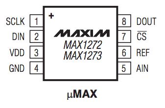
MAX1272 Pinout (Datasheet)
As previously mentioned, we needed an external 12-bit ADC to convert the X and Y channel sinusoidal signals into digital values we can use for our measurements and calculations. The MAX1272 requires a 5V power supply so we could not directly interface it with our PIC32 microcontroller. We obtained a 3V - 5V level shifter, the "Adafruit 8-Channel Bi-Directional Logic Level Converter" (a breakout board for the TI TXB0108). In order to use SPI to talk to the ADC, we had to correctly configurate the SPI hardware for compatibility with the MAX1272. We chose to use SPI channel 1, since channel 2 is used by the TFT. We wanted the microcontroller to be the master, the samples to be taken in the middle of the clock cycle, the clock polarity to be active-high, idle-low and the data out to be clocked out on falling clock edges.
We map the SPI 1 Data In to RPB5 and SPI1 Data Out to RPA4 using PPSInput and PPSOutput, respectively. We initialized it in 8-bit mode, Master mode, and set it so new data came in on rising clock edges. We used a baud divisor rate of 32 in order to get the serial clock running at 1.25 MHz (40/32 MHz). For the MAX1272, the max frequency for the serial clock is 1.4 MHz. Finally, we assign slave select I/O for each device: RPB4 for the first, and RPA3 for the second.
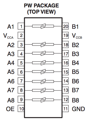
Adafruit 8 Channel Bi-Directional Logic Level Converter Pinout (Datasheet)
We wired SCK1 to shifter 1, RPB5(SDO1) to shifter 2, and RPA4(SDI1) to shifter 3. On the other side were the ADC's SCLK, DIN, and DOUT pins, respectively. The reference implementation required a 1uF capacitor between VREF and GND. We also put a decoupling capacitor with 0.1µF across each level shifter power supply and ground. We tie OE (output enable) to 3.3V with a pull-up resistor to avoid keeping the shifter pins in a high-impedance state. When we tried to connect the CS pins to a channel in the logic level converter, it curiously would not produce any signal on the other side of the channel. We instead made our own one-way inverting level shifters using 2N3904 transistors in a low-side switch configuration with a resistor, where the output is at the collector.
User Interface Hardware
Enclosure
Lab equipment must be well-protected and neatly packaged. We designed an enclosure which could be quickly laser-cut and assembled. We leveraged the engraving functionality to automatically include labels for all UI elements. The material is 1/8" "hardboard" (this one being a lighter variety than the commonly known Masonite).

Front plate as it appeared in software prior to laser cutting. Solidworks used for mechanical aspects, and Inkscape used for UI alignment, labels, etc.
Buttons & Switches
A rocker switch at left opens and closes the PSU's enable circuit, turning the device on and off. Four buttons at right allow for recording null vectors and resetting peak hold. They are wired with one terminal leading to ground, and the other to pins configured for change notification interrupts and internal pull-up enabled. These buttons came in a pack of 5 for less than $2.50.
Signal Connectors
The connectors at left are standard female BNC connections of the type universally used for oscilloscopes, function generations, and the like. They are mounted through the front panel with a nut. The cases have solder tabs on them, which are chained together and grounded to the circuitry. Wires are soldered into the pins, and connected to the appropriate input/output points in the circuit. These connectors came in a pack of 10 for about $10.
Screen
The screen is a PiTFT previously used in another project. We used it because of its larger size and mounting holes, and did not use its touch or memory capabilities. It is completely compatible with Tahmid's PIC32 port of Adafruit GFX, making software and wiring trivial. We used SPI2. It required 5V for its backlight.
Gain Potentiometer
On the right side of the enclosure, we installed two panel-mount linear potentiometers with small knurled knobs. These are each connected to internal ADC pins on the microcontroller (AN4 and AN5) and periodically sampled. Their value is rounded to even digits of a proximeter gain value, which sometimes needs to be calibrated by the user.
Serial Interface
To provide the user with convenient access to serial-over-USB, we connected the UART's TX pin to an FTDI adapter, which we in turn kept connected to a short cable with a panel-mount USB-B socket. The user can then plug any regular "printer cable" into the back of the device for access to data over serial.
Annotated Photograph of Hardware

Code Overview
The code is well-commented and any details should be covered in the source itself. However, we'll say a few words about the "big ideas."
Code Organization
Each major "chunk" of functionality covered below is sequestered into its own header file included near the top of the main program after all global variables have been declared. This is a little sloppy, but illustrates that each file is tightly tailored to this project's purpose. Each peripheral or subroutine has an initialization function as well as some periodic functionality, whether the be a thread or a timer interrupt.
Threads
Non-critical tasks are executed in Protothreads threads. There are only 3 such tasks: updating the graphics with global variables, polling the gain knobs for new gain settings, and sending out serial transmissions containing measurements (also stored in global variables).
The GUI update is a particularly large and tedious piece of code. Fortunately, most of it is completely parametrized, which made calibration easier.
"Per-Sample" Tasks
This file contains tasks running at 8 KHz in a timer overflow interrupt, which primarily consists of the SPI transactions with the ADC. A function pulls the CS signal of a specified ADC low in order to validate the control byte. We write the byte 0b011110001 in order to run the MAX1272 in ± 10V bipolar mode with an internal reference. The code waits for the write transaction to clock out out and the read buffer to fill up before it reads. It takes 3 consecutive 8 bit reads in order to obtain the full 12-bit conversion. We repeat the previous sequence, but write 2 dummy bytes to the ADC to get the SPI clock to run for the transactions. Since it’s in bipolar mode, the numbers returned are in two's complement. The first 8 bit reads are all zeros; the second bit contains a leading zero and the MSB to the 5th bit; the last read contains the 4th bit to the LSB and 3 zeros. After we obtain all 3 reads, we left shift the 2nd read 8 bit, or the results with the 3rd read and right shift the newly obtained 2-byte word 3 bits.
Once we have reads, we implement the peak detection filter discussed in High Level Design. If a peak is found, we also record the phase at which it occurs. We make a special provision to always accept a read if it is the first of a cycle, which occurs when the peak tracking variable amp_meas_[xy] is set to 0.
In all of this, the null vector is also being handled. Phase is always calculated for each sample, and with it the index into the null vector table. If the null vector record flag variable is set, the null vector table is written. If not, the null vector table is read and subtracted from the measured signal.
"Per-Cycle" Tasks
As discussed in High-Level Design, we use Timer23 in conjunction with an input capture unit to measure RPM. Since the input capture interrupt triggers at the end of each cycle (and thus beginning of the next), we use this interrupt to record the result of the many SPI transactions performed during the cycle. Because knowing RPM is critical to phase and null vector calculations, we filter it with a 3-point median filter. RPM and phase measurements are left unfiltered, since they are provided raw over serial, allowing the user to filter the values with host software as they see fit.
Buttons
Code for buttons is worth mentioning simply because it makes use of the change notice interrupt, which is not well documented in any way. Ultimately, we were able to piece it together from a forum post and looking at the PLIB source. After things are all set up, operation is simple - set/clear null vector flags, or reset peak hold values to zero based on what button is pressed.
Construction, Testing, & Results
Construction
Part 1: Signal Conditioning
Construction of the signal conditioning circuitry was remarkably uneventful and proceeded as planned. However, there was some interesting 60 Hz noise on the trigger output which took small ~300 mV square notches out of the trigger waves. 60 Hz implies mains AC interference, but square noise at a fraction of the signal amplitude was bizarre and never explained. The problem occurred when testing on a function generator, but never reproduced itself when running on a real proximeter signal.
Part 2: ADC on Separate Breadboard
When we ran the MAX1272 ADC on a separate whiteboard for testing we ran into a few errors. At first we saw that the chip was sinking current from the CS signal. We initially addressed this with the BJT-based level shifters. In one case, we still had a strange signal on the ADC's CS pin, and tried using another ADC. We found that the first ADC we had been using was damaged for unknown reasons. Potentiometer readings on this new ADC initially seemed accurate, but misbehaved when measuring a ± 5V sine wave. We realized this was simply a string formatting error; after this, the samples showed a smooth transition between about -1024 to 1024 for ± 5V.
Part 3: Integration
After we figured out how to interface the MAX1272 with the PIC32 via SPI, we tried integrating the ADCs with the main circuit. After we re-wired the circuit on the larger breadboard, we tried testing the functionality of our DVF. The ADC would read accurate values maybe once or twice every six to seven samples. We thought this might be a noise problem with the power supply so we placed a .01µF capacitor across the row with the wire from the 5V power supply and GND. This seemed to reduce some of the bad reads from the noisy power supply. The software peak filter was able to compensate for this. We again ran into issues when attempting to add a second ADC in parallel to the first. While we never found the cause, thoroughly re-routing and organizing the circuit out of frustration ended up solving the problem.
Part 4: Final Touches
A piece of MATLAB software was written to read and plot serial communication from the cuDVF. The final microcontroller feature to be implemented was null vector subtraction. We compiled and uploaded "theoretically working" code, and the device continued to operate normally - but, since we do not produce a compensated waveform, we have no way of verifying that the null vector routines are working, or of debugging functionality for further development. This ended up being the biggest "gotcha" this project had to offer.
Testing
To test our device, we set up the full-fledged experiment and wired our device in parallel with the DVF3. We simultaneously plotted data from the DVF3 using a plotting emulator alongside serial data from the cuDVF capture by a MATLAB GUI written for this purpose. We also connected an oscilloscope to observe the time-domain characteristics of the proximeter and cuDVF signals.


Results
Signal conditioning worked well. A scope plot of medium-RPM signals follows. Accuracy of frequency measurement appeared to be "right on" at all times.

The green channel is a proximeter signal, while the blue signal is the signal after offset removal and inversion. The yellow signal is the large negative keyphasor signal, with the red signal being the resulting 0 - 3.3V square wave.
Accuracy of amplitude measurement was difficult to quantify due to lack of non-instantaneous numerical data from the DVF3, but the two boxes appeared to be within 15% of each other, as evidenced by the peak hold comparison below.

Comparison of peaks held: 1780um at 2494 RPM for cuDVF vs. 1711um at 2375 RPM for DVF3. Note that the DVF3 plot is missing measurements at 2500 RPM, so we have reason to believe that the cuDVF performed better.
The final test was a full up-and-down sweep of the rotor with side-by-side plotting. Because the DVF3 does not produce any data other than a graphical plot, statistical performance measures cannot be calculated - but you can see for yourself that the two produced very similar Bode plots and picked out many of the same features in the frequency response.

The cuDVF plots are at left, while the DVF3 plot is at right. Note that the cuDVF produces data points, while the DVF3 attempts to draw smooth lines and "gives up" if it is unsure, such as at the top of resonance.
Conclusion
Results vs. Expectations
Overall, the project was a success. The most obvious shortcoming was the development roadblock on the null vector capturing front, but this provided inspiration for how one might design a more robust version of our device. If we were to design another iteration, it would make use of two microcontrollers: one for full-time null vector compensation/signal processing, and the other managing measurements and user interface processes. To more accurately read phase and amplitude, we would make use of a peak-hold circuit resetting at the end of each cycle, with an added comparator to detect increasing voltage conditions for phase measurement using an input capture module.
Standards
No standard came into play during design, since our goal was to make a proof-of-concept clone of a device used primarily for education and training.
Intellectual Property
Although a thorough patent search would be required prior to embarking on a commercial venture with this product, a cursory search suggests that Bently-Nevada owns no protective patents on the technology. Even if they did, the term of patent is almost certainly expired. Bently-Nevada does however appear to be active in proximeter-related patents, which shouldn't be a problem since we merely interface with these sensors and do not replace them. IP is the only legal consideration related to this project, since measurement of shaft vibrations is not a particularly hot area of government regulation.
Ethical Considerations
As an educational product, the device's purpose can be said to be inherently ethical. Moreover, since it only observes (and does not drive) dynamical systems, it carries virtually no risk of injury. The biggest ethical consideration is that in the event of large-scale distribution, the device must be made absolutely robust and electrically safe for interfacing equipment. Damage of proximeters, for example, could result in hundreds or thousands of dollars of equipment costs incurred by the educational institution.
Notes
An interesting observation made during high-frequency tests was that the device handles chaotic or unmodeled dynamics in an interesting way. Consider the following signal, produced around 3500 RPM:

This appears to be the superposition of two sinusoidal responses, one larger than the other. The DVF3 plot registers the amplitude as somewhere between the two. The cuDVF shows something different:

You can see that at 3500 RPM, the data points jump between two amplitudes - a large one and small one. This is indication that the device is working exactly as designed; amplitude is being measured on a per-cycle basis, with some of the cycles featuring small peaks, and some of them featuring the larger peaks. Cool!