|
| Introduction |
The CCDImager is an Atmel Mega32 microcontroller driven imaging system that uses a Charge-Coupled Device (CCD) optical sensor to capture a still image.
The purpose of this project was to design a basic imaging device from first principles. While brainstorming for ideas for the final project, we came across several varied applications of microcontrollers, from music synthesis and processing to wireless communication. Going through several previously implemented ideas, we noticed that the use of the Atmel Mega32 microcontroller for imaging had not yet been attempted. After further research, we realized that fast, inexpensive and digitized imaging using the Mega32 is possibly among the harder, and hence more interesting applications of microcontrollers. This turned out particlarly true given the processing speed limitations of the Mega32, the budget constraints of this project, and performance limitations of common analog hardware parts at high frequencies. To be able to contend with these limitations and develop a reasonable product, our goal was to gain as much exposure to hardware design concepts as possible, as well as utilize the AVR architecture, C and assembly language abilities we had developed in this course.

|
| High Level Design |
The source of inspiration for our project was a dirty old Epson scanner that we stumbled upon in our dorm. Since any scrap parts we gathered were not counted in our budget, we had been collecting any and everything that could possibly have been of use. While thinking about final project ideas, we decided to take apart the scanner, and research into how it works. The online literature indicated that several scanners use CCD image sensors, and further reading sparked an interest in CCD sensors.
After a detailed search, we decided to use Texas Instrument's TC237B CCD Image Sensor, since it has good resolution (680x500 pixels), scope for anti-blooming, high sensitivity, and NTSC compatibility, which would ease adaptation to video applications. The TC237B has an internal structure that converts the charge stored in its charge wells due to incident light, into voltage at 12µV per electron. This voltage is transferred out from the CCD by sending it a series of pulses for row and column transfer. These will be described in detail later.
In order to be able to process the CCD's outcoming voltage signal, a high speed digitizer was necessary. This digitizer, often referred to as the "analog front end," acts as a fast ADC, with an inbuilt structure that is particularly useful for digitizing CCD voltage waveforms. The Analog Devices AD9822 seemed like a good choice because it has a 14bit, 15MSPS ADC, and is specific to CCD applications.
The Atmel Mega32 has an onboard 2KB RAM. However, for digitizing the 340,000 pixels of the CCD sensor at 2 bytes/pixel, this was highly insufficient. As a result, we decided to use an external SRAM to store the digitized output of the AD9822, and then transfer it into the Mega32 from this internal memory. We chose Cypress Semiconductor Corporation's CY7C1048CV33, a 4MB (512 x 8) Static RAM chip, because of its ease of control due to TTL-compatible inputs and outputs, low power usage, high speed, and its generous storage capacity.
The high-level circuit diagram is shown in Figure 1:
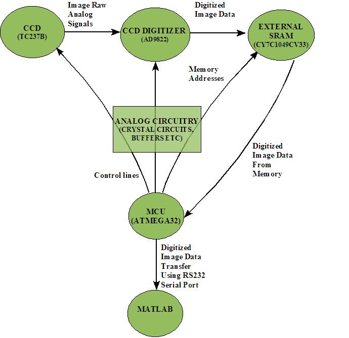
Figure 1: Overall High-Level Design of CCDImager
|
| Hardware Design |
The first concern in hardware design was the design of a circuit to provide the necessary voltage signals and swings to the CCD sensor. As a first approach, we studied the datasheet of the TC237B CCD sensor in order to see what circuit would fulfill the necessary specifications. However, the "Recommended Operating Conditions" specified by the datasheet required voltage levels up to 26V. This was beyond what the voltage supplies available in lab could provide. As a consequence, we tried looking into making our own voltage supply circuits using voltage regulator chips and a 30V power supply we were able to borrow. However, this proved to be a rather daunting task as we required at least seven different voltage levels for the CCD to operate properly, and this would have meant that a lot of hardware resources (solder boards and so forth) would have been taken up by just the voltage supply circuits. In addition, the couple of test circuits we attempted did not hold very regular voltage levels. After seeing these disappointing results, we decided to look at the online literature for information on alternate implementations of the CCD voltage levels. There seemed to be major differences in the various literature we studied. In the end, we decided to implement the circuit provided by Texas Instruments in the CCD datasheet under "Application Information," even though the voltage levels suggested in that circuit did not agree with their own "Recommended Operating Conditions." This circuit is shown and explained below.

Figure 2: Circuit to Drive the TC237B CCD Image Sensor (Image from the TC237B Datasheet).
The CCD sensor requires the following signals: CCD_ADB, CCD_SRG, CCD_RST, CCD_ODB, CCD_IAG1, CCD_IAG2, and CCD_SAG. The CCD_ODB provides an overflow drain bias for anti-blooming the charge wells so that there is less smear between neighboring pixels. An application of a minimum 1µs pulse on this signal sets the clearing and integration phase in which charge is collected on the charge wells. The CCD_IAG1 and CCD_IAG2 signals provide the voltage to drive the image gate areas 1 and 2 respectively. In progressive-scan timing with single register readout (the mode we implemented), the CCD_IAG1 and CCD_IAG2 signals are tied together. The CCD_IAG signals, along with the CCD_SAG (for the storage area gate), drive the collection of charge in the charge wells and its parallel transfer from the image area to the storage area. The CCD_SRG signal then begins the serial transfer of the charge out from the storage area, onto the output pins CCD_OUT1 and CCD_OUT2. The CCD_RST then resets the gates during serial readout. The CCD_ADB signal is the supply voltage for the amplifier drain bias. This means that the CCD is effectively on when this voltage is supplied. As a result, this signal is at its high value during the course of the above mentioned steps of exposure, integration, parallel transfer to the storage area and serial transfer out of the storage area. The MAX333A single-pole double-throw (one control line for two selectable lines - three way switch) was used to switch the CCD_ADB signal on and off since it is very fast and can handle large voltage swings. The CCD datasheet recommended a frequency of 12.5MHz to drive the CCD_SRG, CCD_RST, CCD_IAG1, CCD_IAG2, and CCD_SAG signals. However, our tests for the crystal oscillator circuits for the 12.5MHz and 5MHz showed that the 12.5MHz signals were much more noisy than the 5MHz signals, so we tried using a 5MHz frequency for these signals. This succeeded in driving the circuit, so we made a design change from 12.5MHz to 5MHz for these signals. The crystal oscillator circuit is described later. All voltage signals to the CCD are in reference to the CCD_SUB (substrate) voltage, which is connected to ground in this implementation. The desired signals for the progressive-scan timing with single register readout mode is shown in Figure 3:
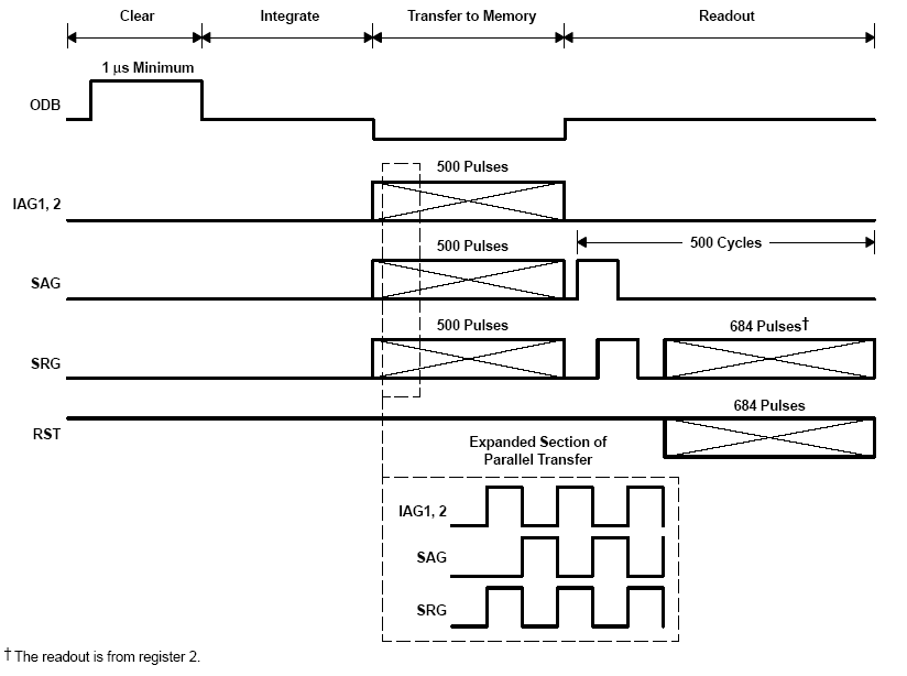
Figure 3: Voltage waveforms for the CCD: Progressive-scan timing with dual-register readout
(Image from the TC237B Datasheet).
The circuit in Figure 2 is thus divided into three main parts: (1) Serial Driver, (2) ODB Driver, and (3) Parallel Driver.
(1) Serial Driver Circuit
In our execution of the serial driver circuit, we implemented the PMOSFET switches with the npn TIP31 transistors, and the NMOSFET switches with the pnp TIP32 transistors. For the diodes in the figure, 1N914 diodes were used. The generation of the SRG_CLK and RST_CLK signals is described in the Interface Design section. Once these signals are obtained by the serial driver circuit, they are put through a tri-state octal buffer (74ACT240NS), which inverts the incoming SRG_CLK and RST_CLK signals, and also helps restore the incoming signals to TTL logic levels if they were attenuated by noise. The alternate high-low nature of the signals coming out of the 74ACT240NS buffer alternate which transistor (TIP31 or TIP32) is on, and therefore switches between the 2V and -10V supplies.
(2) ODB Driver Circuit
The npn transistors in the ODB driver circuit were implemented using 2N3904 npn transistors. When a TTL logic high signal is sen on the ODB_CLK line, the 15V supply is selected by the pair of npn transistors. When the ODB_CLK line carries a logic low, CCD_ODB switches to the ground-level voltage of 0V. The ODB_CLK signal is generated by the microcontroller. This is described in the Interface Design section.
(3) Parallel Driver Circuit
The Toshiba HN1A01F dual epitaxial general purpose transistor chips are no longer produced, so we used an equivalent chip, the IMT1AT110. Again, the generation of the IAG1_CLK, IAG2_CLK and SAG_CLK are described in the Interface Design section. Close inspection of this circuit reveals that since the emmiters of the transistors are shorted and taken to 5V supply through a resistor, there is a voltage divider between the 5V supply anf one of the bases, and the collector on one side is taken to the low voltage of -10V, the construction is that of a current mirror. This is to make an ad-hoc scheme for amplification of the incoming signal. Transistors can switch at frequencies up to 100MHz, and this provides a convenient way of achieving amplification that would have been impossible to implement with other relatively slow amplification methods such as using op-amps. This amplified signal is then fed into the EL7202C non-inverting high-speed power MOSFET driver. This chip regulates the relative phases of the CCD_IAG and CCD_SAG waveforms so that they are fed to the CCD one cycle out of phase, as seen in Figure 3.
The memory and CCD digitizer circuits were constructed according to their datasheets and as described in the Interface Design section. Again, we found that the lesser noise carrying 5MHz frequency worked with the CCD digitizer, so we made a design change to switch from 12.5MHz to 5MHz.
Crystal Oscillator Circuits:
For the crystal oscillator design, we referred to the following circuit:
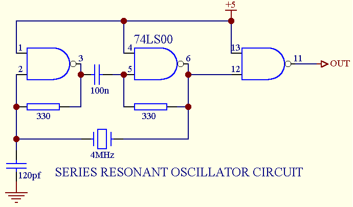
Figure 4: Crystal Oscillator Circuit (Image from Thomas Scherrer Crystal Oscillator Circuits).
The capacitance that sits near ground, along with the 330Ω resistor, determines the cutoff frequency for the circuit, according to fc = 1/(2πRC). With R constant at 330Ω, we get C ≈ 88nF for 5MHz, C ≈ 33nF for 12.5MHz, C≈29nF for 15MHz crystals such that the cutoff frequencies are just above the respective desired frequency.
Testing:
Once every component circuit was built, it was thouroughly tested with a variety of signals and timing combinations, and the output was observed. Several circuits, like the crystal oscillator circuits, had to be fine tuned with regards to capacitances and resistances, until a predictable and stable output was obtained. For sanity checks, we built the different component circuits in PSpice when possible and checked the real output against the model simulations. The recorded outputs agreed with the PSpice simulation results quite satisfactorily when tested individually, and then the design of that component circuit was finalized.
|
| Interface Design |
One of the major tasks in this project was to interface all the hardware with each other and implementing the ATMega32 as the controller of all the control lines involved in this interfacing. This part of the project took the bulk of our time. The signals such as IAG1_CLK, IAG2_CLK, and SAG_CLK had to be generated at 12.5 MHz according to the specifications of the CCD sensor. The SAG_CLK is a delayed version of the IAG1_CLK and IAG2_CLK. To accomplish this delay, the ATMega32 was disregarded immediately as it can generate a clock signal of only 8 MHz. This lead to only one choice, which was implement these signals in hardware. The entire project is pretty much running on a high frequency, therefore, most of things were implemented in hardware, and the software was traded off for hardware.
The block diagram of the entire circuit can be found in the Appendix. Crystal oscillator circuits are shown merely by the crystal symbol in this diagram for simplicity. For the oscillator circuit, refer to the Hardware Design section.
The ATMega32 just controlled when these signals would be on or off at the right time. PORTB pins were used to achieve this. We found out that the 74LS240/241 chips are octal tri-state buffers which have switching time of 10.5ns to 12ns. The enable signals, which are usually active low, for these buffers were generated by the PORTB pins as outlined in the block diagram below. In the block diagram, the crystals are shown as separate entities, but it is just two crystals running the entire thing. The crystals required a crystal oscillator circuit to make it stable; this is described in the Hardware section of the report. We made the decision to make the control line for IAG1_CLK, IAG2_CLK, SAG_CLK, and SRG_CLK active low because it will enable to turn on the buffer chip easily without having to invert the enable signal. The pin B.2 is the control line for the IAG1_CLK, IAG2_CLK, and SAG_CLK, which enables the tri-state buffer. These IAG1_CLK, IAG2_CLK, and SAG_CLK signals act as inputs into the parallel driver circuit, which is described in the “Hardware Design” section. Pin B.3 acts as the SRG_CLK control line, and this was implemented using a NAND gate (74LS00) as the CCD sensor requires a SRG signal when IAG signals are on during parallel transfer mode, and also SRG can be on independently during serial transfer mode. The output of the NAND gate became the enable for the buffer chip, so the SRG_CLK signal could be outputted. The input into the buffer chip was the clock signal that was required to drive the supporting analog circuits for the CCD sensor. Texas Instruments recommended to use 12.5 MHz clock signal, however, the 12.5 MHz signal generated an incredible amount of noise, and subsequently, CCD sensor outputted noise. Therefore, we stepped down to a 5 MHz signal before demo day. Most of the discussion in this report is based on the 12.5MHz clock for the CCD sensor and the 15MHz clock for the AD9822, CCD signal processor. Pin B.4 controls the RST_CLK signal, which is used in the serial driver circuit along with SRG_CLK signal. This control line is active high. Each octal tri-state buffer chip has two enables, and SRG_CLK, IAG1_CLK, and IAG2_CLK is housed on the 74LS240, while the 74LS241 housed the SAG_CLK and CDSCLK1 signals. Since we were running out of space on the solder-boards, we had to implement the RST_CLK using NAND gates from 74LS00 chip. Basically, the crystal is plugged as one of the inputs into the NAND gate, and the other input is B.4, this gives an inverted RST_CLK signal, therefore, another NAND gate is used to invert this signal to get the correct RST_CLK for the serial driver circuit. Pin B.0 is used to generate the active lwo ODB_CLK signal which when it is held low for more than 1µs clears the charges accumulated on each pixel on the CCD sensor. This ODB_CLK signal is implemented by the microcontroller and this signal feeds directly into the ODB driver circuit. In software, these control lines are manipulated to give out the “single register readout” through the pin OUT2 of the CCD image sensor. This output signal from the CCD sensor is a correlated double sampled signal or CDS signal. CDS sampling is discussed below. The waveform in Figure 3 describes the parallel transfer mode, and serial readout mode for the TC237B image sensor.
For parallel transfer to memory mode, one can see that IAG1, IAG2, and SRG are in phase, while SAG is delayed or inverted. This is why SAG_CLK is housed on the 74LS240 inverting octal tri-state buffer. The enables of IAG1_CLK, IAG2_CLK, and SAG_CLK are coming from the same pin. Consequently, the only delay that will be present in the signal is the 10.5-12ns gate switching delay. However, the enable for SRG_CLK goes through a NAND gate causing a delay of 10ns for the SRG_CLK. But this was ignored, because the period of the 12.5MHz signal is 80ns. For the serial readout mode, the following waveform was required to be generated:
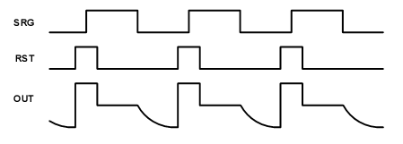
Figure 5: Serial Readout Mode
This is where SRG is running at 12.5MHz, and RST signal is pulse that is high for the rising edge of SRG. It is clear that RST is not high for the falling edge of the SRG. This means we need control of RST pulse for a maximum of every 40ns or less, but this is not possible to implement using the Mega32 since it takes 62.5ns to complete one instruction. Subsequently, the RST signal was implemented in hardware by making RST_CLK and SRG_CLK out of phase by one NAND gate, 10ns, and one instruction, 62.5ns. This means that if SRG_CLK was started before RST_CLK, then 7.5ns of the low SRG_CLK will be left at which the RST_CLK will be enabled, therefore making them out of phase. A waveform is shown below in Figure 6.
Figure 6: Timing for the RST_CLK and SRG_CLK signals
The above waveform, according to the datasheet, should give out a CCD output signal. However, this wasn’t the case and we switched to the value of 5MHz, but there is still adequate noise generated by the driver circuits that the signal going into the CCD sensor may not be the desired waveform.
Since MATLAB is used in this project, D.0 and D.1 are jumped for the recognition of the RS232 transfer. The CCD signal processor, AD9822, can handle 3-color CCD output signals. However, TC237B is a B&W image sensor, therefore, the AD9822 needs to be switched into 1-Channel CDS mode. The AD9822 digitizes the analog input, the CCD sensor’s output, into a high byte and low byte. The high byte will be stored to external SRAM because the low byte doesn’t give an accurate digitized value for the CCD sensor. Thus, SLOAD and SDATA are used to hold the internal multiplexer in a fixed state. The SLOAD is located on pin D.5 and is active low. The SDATA pin is B.2 and in software, the appropriate bit stream for changing the settings of the AD9822 is delivered to the serial interface of the chip. In addition, the SCLK for the serial interface is hooked to the AD9822’s ADCCLK. The output of the CCD sensor is plugged into the VINR pin of the AD9822, which is the analog input for the chip during 1-Channel CDS mode. To get an output from the AD9822, the active low OEB signal should be set low. This signal is located on pin D.6. The ADCCLK, along with the CDSCLK1 and CDSCLK2, is used for digitizing the analog signal outputted by the CCD sensor. The AD9822’s CDSCLK1 samples the reference signal of the CCD waveform on its falling edge, and CDSCLK2 samples the data level of the CCD waveform on its falling edge. This is CDS mode. The timing waveform for the AD9822 1-Channel CDS mode is shown below in Figure 7.
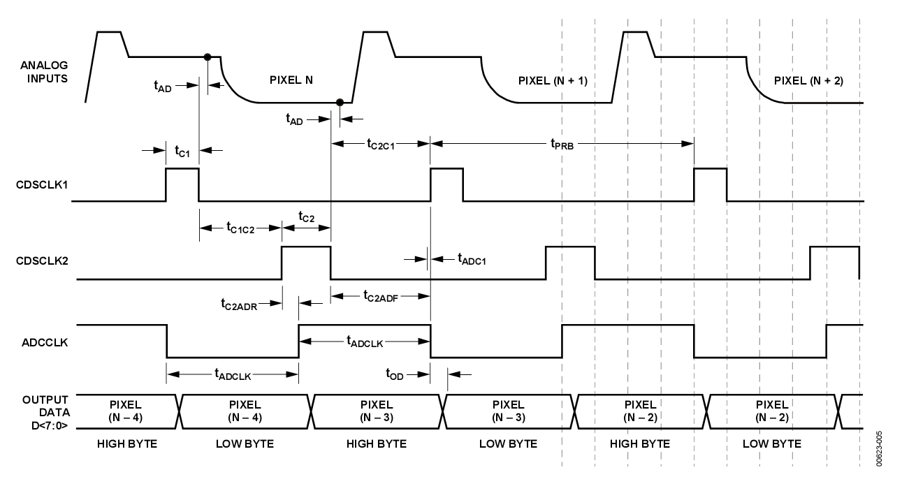
Figure 7: Timing waveform for AD9822 1-Channel CDS Mode (from AD9822 datasheet).
In this diagram, the pulse width of CDSCLK1 and CDSCLK2 is 10ns, and ADCCLK is running at 15 MHz. One can notice that the high bytes are outputted when ADCCLK is high, this note will be used during SRAM transfer. The datasheet for AD9822 says that the CDSCLK1 and CDSCLK2 are connected to the 5 MHz crystal. However, a clock signal will make the pulse width large. The Mega32 cannot generate the CDSCLK1 and CDSCLK2 for the reason that it will take 62.5ns to toggle a bit on the port. Also, after carefully reading the datasheet, two major errors were found. The value of tC1C2 given by the datasheet is 0 and value of tPRB is given as 80ns. But, when you account for all the values given – tC2, tC1, and tC2C1, things don’t add up.
tPRB = tC2 + tC1 + tC2C1 + tC1C2
80 = 10 + 10 + 40 + 0
There is a discrepancy with the given value of tC1C2 being 0ns. After looking up other CCD signal processors from other manufacturers, we found that tC1C2 should have a value such as 10ns. If tC1C2 is 0, then the waveform shown above doesn’t make any sense because CDS sampling is not even occurring. Another major error that was found in the document was the description of the above waveform. The datasheet quotes, “It is recommended that the falling edge of CDSCLK2 occur coincident with or before the rising edge of ADCCLK… The rising edge of CDSCLK2 should not occur before the previous falling edge of ADCCLK.”
It is clear that the rising edge of CDSCLK2 occur coincident with or before the rising edge of ADCCLK. If the description of the waveform is followed, then it can be shown that the rising edge of CDSCLK2 occurs before the previous falling edge of ADCCLK, and this is not allowed by the datasheet.
To tackle these errors, we followed the waveforms and not the description. Since we can’t generate pulses of length 10ns with a Mega32, we have to do this in hardware. There is no way to generate a 10ns pulse with the hardware at hand. The waveform below shows what would happen if CDSCLK1 and CDSCLK2 were connected to the 5 MHz clock, while the ADCCLK is connected to 15 MHz. CDSCLK2 flows through an inverter buffer, 74LS241, before going into AD9822, therefore, there will be 10ns gate delay from the buffer. CDSCLK2 is enabled by B.3, which is the SRG_CLK active low signal. Since serial readout is happening while AD9822 is digitizing the CCD sensor’s output, it is appropriate for B.3 to act as a control line for CDSCLK2.
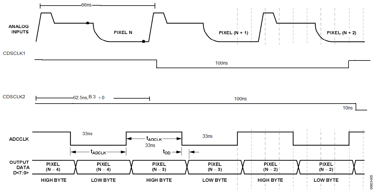
Figure 8: Timing waveform for AD9822 1-Channel CDS Mode with 15MHz as the frequency ADCCLK
If the waveform was extended to include more cycles, it can be noted that you are skipping pixels. Also, since we made T237B signals to run at 5 MHz, the above waveform ADCCLK running at 15 MHz, and it will mess up the digitized value from the analog input. Thus, we had to come up with a waveform that would decently produce CDS samples. From the datasheet it is not necessary for CDSCLK1’s falling edge to be during the reference but the falling edge of CDSCLK2 has to be during the data section of the analog input. The waveform below is what was implemented.
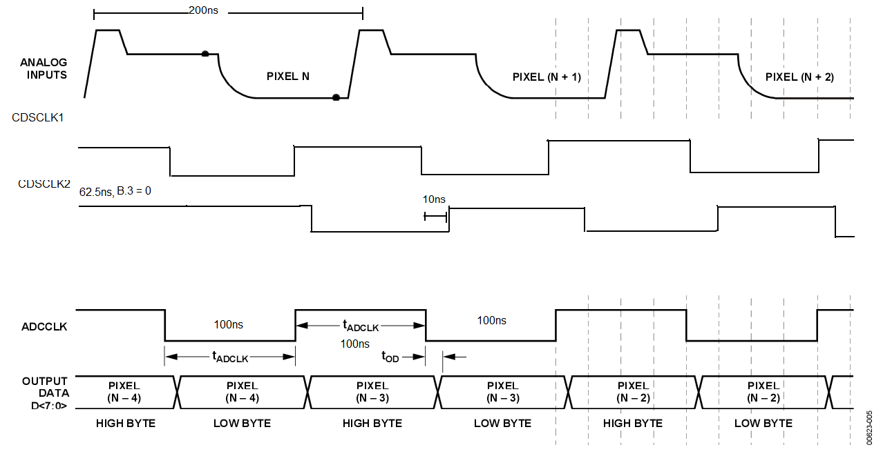
Figure 9: Timing waveform for AD9822 1-Channel CDS Mode with 5MHz as the frequency for ADCCLK
In the waveform in Figure 9 above, we can see that every pixel is correctly sampled using the CDS technique. Although 100ns is greater than 62.5ns, the Mega32 can toggle a bit but getting a 200ns period is still difficult, because the period has to be in multiples of 62.5ns.
The output of the AD9822 is in the form of high byte and low byte for the high ADCCLK and low ADCCLK respectively. The high bytes need to be stored in SRAM. The Mega32’s SRAM is only 2Kbytes, which is very inadequate, as 340000 pixels on the CCD image sensor will yield 340000 high bytes from the AD9822. Henceforth, an external SRAM memory chip was used. The memory chip, CYC1049CV33, is an asynchronous SRAM organized as 2048 x 256 bytes. This memory chip has three active low control signals: CE, OE, and WE. The signal CE, D.2, is set to low to turn on the memory. Since the high bytes are outputted when ADCCLK is high, but WE is active low, therefore, we connected the WE to CDSCLK2. The data output bits - D7...D0, from the AD9822 is bused to the I/O pins of the memory. The addresses for columns and rows are generated by the microcontroller. D.7 is used as the MSB of row addressing. All the pins in PORTC are dedicated to row address generation. All the pins in PORTA are dedicated to column address generation. The high bytes are stored into memory as a matrix of 443 x 255. These dimensions were chosen because the address generation code skips a few high bytes because of instructions time to execute the increment of the address and output the incremented address to a port. After all the elements in the 443 x 255 matrix are filled, then it is time to read the stored values in the memory. Since PORTA and PORTC are dedicated to address generation, this leaves PORTB and PORTD to get the data from the memory. PORTD is used for controlling memory signals, therefore, PORTB is used. However, PORTB houses control signals for the CCD image sensor. If PORTB is connected to the memory I/O pins, then during write stage of the memory, the data from the AD9822, which goes into the I/O pins, can affect the PORTB pins. Considering this, a 74LS241 octal tri-state buffer was used to avoid this cross talk. This buffer chip is enabled using the active low OE signal from the memory. The OE signal is located on the D.3 pin. But once this buffer is on, lines going from the buffer to PORTB will talk with the PORTB lines going to the CCD sensor. Subsequently, to be safe, the CCD sensor was turned off using the active low OE signal. A MAX333A chip was used to switch the voltage for the CCD power, ADB, between 12V and GND. When the OE signal is high, CCD is on and CDSCLK2 is on. But, if OE is low, CCD is off, CDSCLK2 is off, and the memory can be read at the Mega32’s pace.
|
| Software Design |
Since most of the functionality of this project required high frequencies, the Mega32 was used to control the hardware and create the waveforms required by the chips. The Mega32 was also used to generate addresses for the memory, which was used to store the output of the AD9822. Once the memory has been written, the microcontroller was used to read from the memory and it then transferred this data to MATLAB, which processed it to create an image. Most of the software was rewritten because we switched to 5 MHz crystals in the last week before demo day.
There are several states that the Mega32 has to control to get an image out of the CCD sensor. The state machine is shown below.
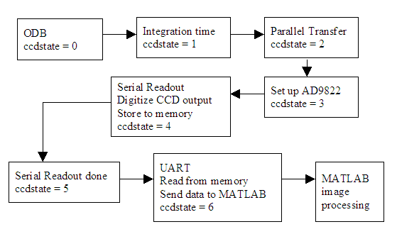
Figure 10: State Machine for the CCDImager
Timer0 compare match interrupt was used with different OCR0 values. The OCR0 values were dependent on the state required for the CCD sensor. For instance, the state of “integration time” requires anywhere from 1µs to 30µs , and then OCR0 was set to 250 to give around 15µs. Timer0 was run at 16 MHz. In the ODB state, B.0, the ODB_CLK pin is set to low, which is connected to the ODB driver circuit, and clears the CCD sensor. In parallel transfer mode, the SRG_CLK, SAG_CLK, IAG1_CLK and IAG2_CLK are set to give out the 500 pulses and accordingly, timer0 is used to time this state. The setup for the AD9822 requires changing the configuration registers, which is done using SDATA and SLOAD. Since we are using 5 MHz clock each bit of the serial data transferred from the SDATA pin should be present for 200ns. To do this, 3 nops, each taking 62.5ns, were put in place after each bit of SDATA. The next state is the serial readout. In this state the timing is critical when it comes to which PORT pin should be active first. Several waveforms were drawn, which included the instruction cycle time, and hardware response time such as gate switching times, and thus, SRG_CLK and RST_CLK code was played around with a lot to create the correct phase as required by the TC237B to serially transfer the raw analog data. In the meantime, the AD9822 control lines have been set up to take in this raw analog data and digitize it. The AD9822 was used in CDS mode, thus, the timing for CDSCLK1 and CDSCLK2 was critical in getting the correct values. Again, waveforms were drawn such as shown in the “Interface Design” section. The 62.5ns instruction cycle time is of great importance when it comes to syncing clock signals to produce the waveform required by the chips. If the 62.5ns is too slow, then the activity is implemented in hardware and software is traded off. For example, when the AD9822 and CCD sensor were running at 12.5 MHz, then the address generation for the memory, which would store the digitized CCD output signal was implemented in assembly. Several calculations were done so that only the high byte from the AD9822 was stored to the memory. This involved skipping two or three high bytes. One high byte is skipped for the increment command of the column, and another high byte is skipped for the output of this increment to PORTA or PORTC. But when it was noticed that the CCD clock signals carry a lot of noise, the 5 MHz crystals were used, and this assembly code was removed. Now, a for loop is used to traverse through the memory while storing the output from the AD9822. Once the serial readout is done, the next state turns off all the clock signals being used in the previous state. In the UART stage, memory output enable is set to low. This signal turns off the CCD sensor to avoid cross talk. This is described in detail in the “Interface Design” section. The memory is read using address generation in a for loop, then the output from the memory is read, and transferred to MATLAB at 9600 baud.
The memory has a matrix of 443 x 255 bytes filled with digitized values. A calculation can be made to calculate the time it takes to transfer 443 x 255 bytes.
443*255*8 = 903720 bits
At 9600 baud, it will take 903720/9600 = 94.1seconds
However, this is 94.1 seconds doesn’t take into consideration the wait time for MATLAB to send a character to the Mega32 to request a byte, the address generation, printf() and fscanf() functions. At 9600 baud, 10000 bytes takes about 8 minutes to transfer from external SRAM to MATLAB. Higher baud rates were tried, but the serial COM ports froze.
MATLAB sends a character to Mega32 requesting for a byte of data, the Mega32 generates an address and gets the data from external memory. Then, using the printf() function the Mega32 transfers this byte of data to MATLAB, which uses the fscanf() function to receive this byte of data. This process continues. Finally, after all the data has been received, MATLAB sends a character to the Mega32 indicating that it doesn’t need data anymore.
In MATLAB, the obtained matrix is reshaped to make it square or rectangular. After this, all the values are converted to 8-bit values using the uint8() function. With the color map set to “gray,” MATLAB displays the original image. It also displays a minimized version of the image, which might have been useful for blasting that image on to the TV. Also, a Lucy-Richardson deconvolution filter is used with Gaussian noise of threshold value of 0.5 on the original image to get rid of noise caused by the CCD sensor. It clears up the noise in the obtained image. After this, the deconvoluted image is minimized. Edge detection is done using the Sobel method, which uses the Sobel method of approximating a derivative. Basically, it finds the spots in the image where the contrast is the most and indicates it as an edge. Edge detection is conducted on the original and deconvoluted images to display the difference. The edge detection on a deconvoluted picture often shows more edges.
Software Testing
Software testing was done by drawing several waveforms of instruction cycles and calculating the hardware propagation time of a signal to the appropriate chip. Hyperterm was used to check if all the states were reached. MATLAB array editor was used to see the changing values of data received from the Mega32, which also indicated that the memory was read out and wrote properly. This also pointed out that AD9822 digitized the raw analog output from CCD sensor correctly. Thinking about software made us think about interface design, and this interface design was tested by using software such as controlling lines for clock signals to the CCD sensor, the AD9822, and control lines for buffer chips. This project made us think about how critical timing can be, and if timing is slightly off the CCD sensor will not function appropriately and not give an image. Generating pulses at 12.5MHz was not possible in software; therefore, control lines were created so that an external clock signal can provide the pulses while the microcontroller enabled these external clock signals. The oscilloscope was used to test out if the control lines coded enabled or disabled clock signals at the right moment to provide the pulses or waveform required by the CCD sensor or AD9822. Professor Land’s code for communicating between the Mega32 and MATLAB was referred to and a small test program was created to test out the RS232 serial connection between Mega32 and MATLAB.
Hardware and Software tradeoffs
When the project started out, we were trying to use the recommended conditions for the AD9822 and CCD sensor. The AD9822 required 10ns pulses to sample the raw analog signal synced with ADCCLK and a 15MHz ADCCLK clock signal. The CCD sensor required several 12.5 MHz pulses synced in a certain way for parallel transfer mode, and serial readout mode. All of these signals could not be achieved in the Mega32, as the Mega32 runs at a maximum frequency of 16MHz, which means to toggle a bit up and down, will give a resulting frequency of 8MHz. This is not sufficient to drive the CCD sensor or the AD9822. As a result, every one of these signals had to be implemented in hardware. The Mega32 lacked enough port pins to address the memory, read from the memory, and generate control line signals. This was remedied by using PORTB twice, once as an output for CCD signals and as an input when the external SRAM is read. But software cannot do anything when cross talk occurs between the memory and the CCD sensor when PORTB is changed from output to input. As a solution to this problem, a buffer chip was enabled on and off depending on the direction of the PORTB pins. A control line was used for this buffer chip. The Mega32 comes with 2Kbytes of SRAM, which is barely enough to store the digitized image from the CCD sensor. An external SRAM of 512Kb was used instead. The software was used to generate addresses to this external memory. Some other trade offs between hardware and software are also outlined in the “Interface Design” section.
Pin out for the connections and control lines for the ATMega32 is attached in the Appendix.
|
| Testing and Results |
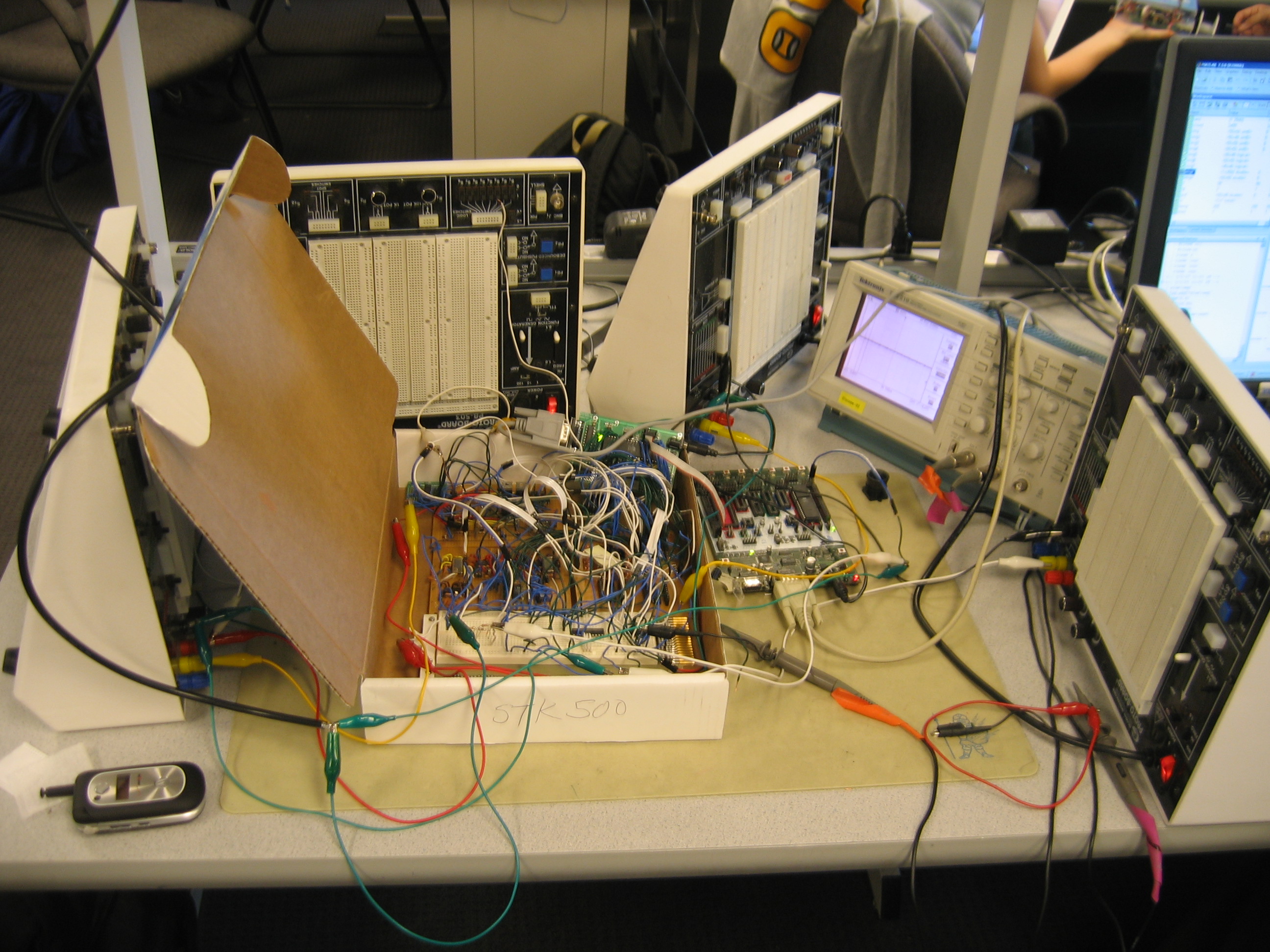
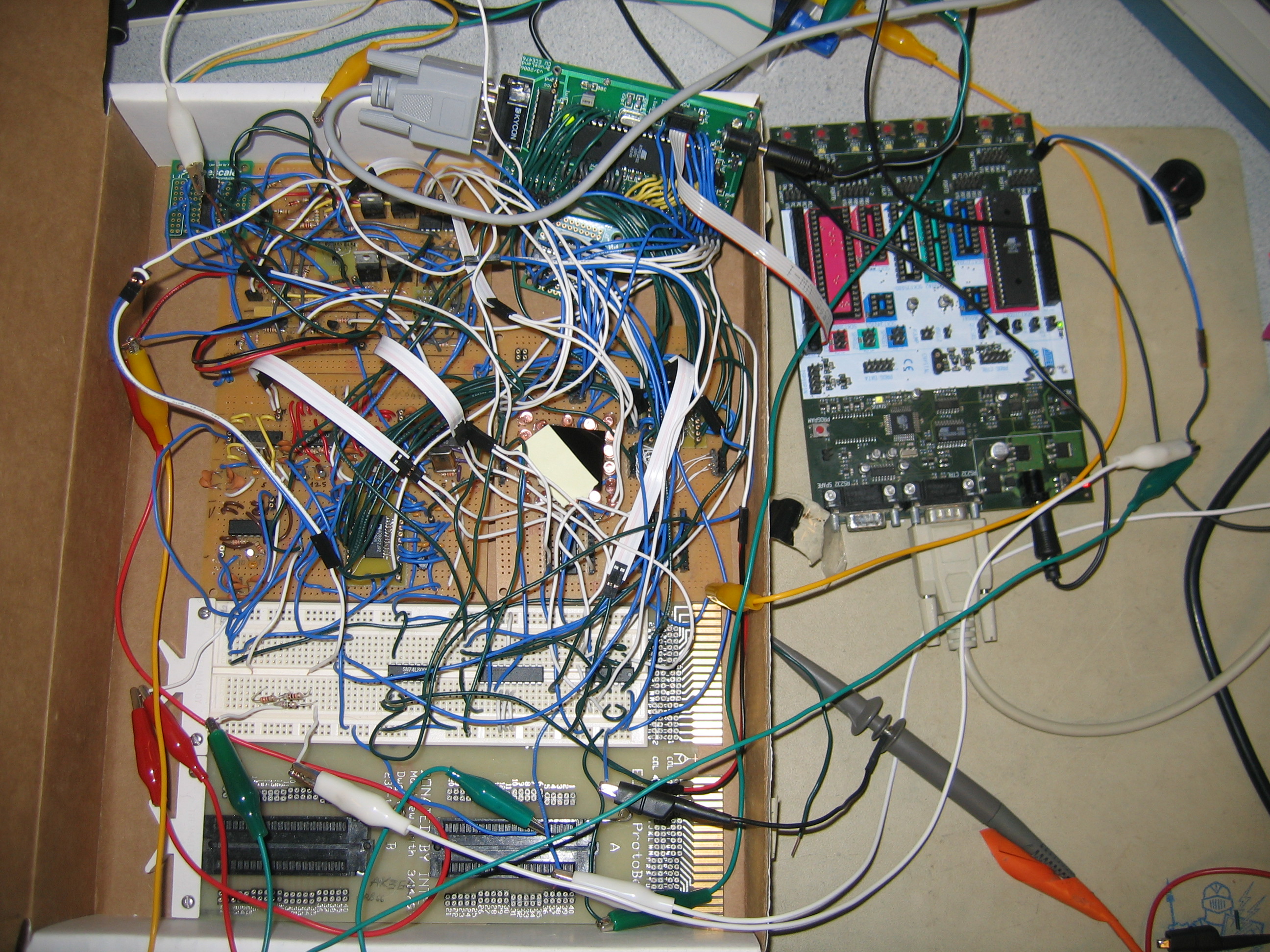
Individual component circuits were thoroughly tested, and once satisfactory results were obtained for each of the component circuits, the entire circuit was put together for testing. At first, we noticed that we were not getting an output signal from the CCD. Checking the various signals that drive the CCD, we found that all the signals were extremely noisy. Even a fleeting glance at the circuit gave away one of the reasons for the presence of this large noise component: our circuit is rather large, and to be able to fit budgetary restrictions, space on the solderboards has been optimized. This has meant long wires running to and from one part of the circuit to another. The more important, and dominating reason has roots at the very basic premise of this project: high frequency. All our circuits run at 5MHz or higher. At such high frequencies, all these long wires start acting like localized antennae and set up significant inductances, causing interference with one another and leading to large amounts of noise. Adding bypass capacitances between the various voltage sources and ground also proved to be a rather futile exercise because of the sheer number and length of wires present, that leads to significant amplification of noise as we get even slightly further away from the point where the bypass capacitance was added. Significant pruning of as many wires as possible resulted in somewhat better signals, although they remained substantially noisy. The number of wires and plug-in connections by itself meant that slight jolts during movement of the circuit, or things as simple as slightly changing the position of the circuit could possibly knock wires loose. This made testing the circuit extremely frustrating, as connections had to be constantly checked and rechecked until decent signals could be obtained.
Another point that complicated getting predictable outcomes was the processing speed limitations of the Mega32. As discussed in the Interface Design section, the Mega32 is not fast enough to control timing effectively so that our signals could follow the prescribed specifications. In addition, the duty cycle of these signals could not be controlled by any simple way without adding a significant amount of components. This, once again, prevented us from generating the prescribed operating signals. This variation, coupled with the noise, inhibited a predictable output signal from the CCD. Moreover, since the Mega32 is not fast enough, transferring data from the external SRAM into the microcontroller and subsequently into Matlab using RS232 serial interface is very slow. We have 443x255 = 112965 bytes in the memory that need to be transferred out. However, transferring 100 bytes takes around 2-3 seconds. This means that transferring the entire data in memory could take up to an hour. As a result, we are forced to transfer only a small chunk of this memory, say at most 10000 bytes, which takes about 8 minutes. Thus, if we are trying to image something, it is easily possible that its data was not in the chunk that we transferred, and hence we were not able to image it. These limitations were in addition to the fact that not all bytes are transferred from the CCD digitizer into the memory. Several bytes needed to be skipped due to speed limitations.
Another source of error for our tests was that we were not able to use a lens and focus the image properly onto the image area of the CCD. Budgetary considerations, and the fact that the hardware is extremely cluttered with wires and delicate connections prevened us from building an additional lens mount.
Despite all these limitations, the noisy and temperamental circuit did give us some very nice results. The following are images that were captured by the CCD and processed in Matlab. In each of the following figures, the top left picture is the actual data captured; to its right is its minimized (resized) image for ease of blasting to the TV (we did not implement this feature); on the top right is the deconvoluted version of the original image. On the bottom left is the minimized version of the deconvoluted image (again, for ease of blasting to TV). The next image is the output of running Matlab's edge detection algorithm on the mimized image; the last image is the edge-detected version of the minimized deconvoluted image.
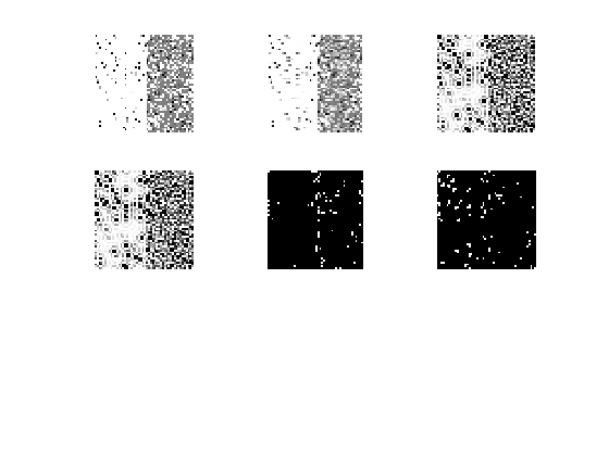
Figure 11: Half of the CCD image area covered with post-it notes, and a desk lamp
held over the CCD.
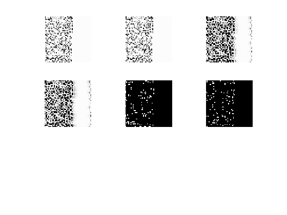
Figure 12: A wire held over the CCD and a desk lamp shining above. Notice the thick
region where the wire was held.
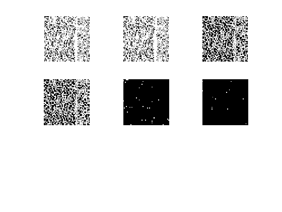
Figure 13: A fine wire mesh kept directly on the CCD with a desk lamp shining above.
Notice the thin band of the fine wire mesh.
|
| Conclusions |
Our basic goal for this project was to use an image sensor and apply image processing techniques on the image received from the image sensor. Hence, both of us came up with the idea of CCD Imager. The hardware of this project required lots of different circuits to drive the different chips we had. The limitations of the Mega32 required us to add additional circuitry in the form of buffer chips and NAND gates. Bulk of the time in lab was used up in interfacing different chips with each other and building the hardware. Since, we had a number of parts, we referred to their datasheets and have become experts reading datasheets. We found a few errors with Analog Devices’ AD9822 datasheet. Also, we learnt that when something is recommended, it is really not necessary to follow it. Chips can be implemented in other ways as well, however, some engineering skill is required in order to not burn the chip. The software controlled the hardware. However, the analog circuits produced a huge amount of noise, often rendering the pulses sent to the CCD sensor useless, and therefore, no picture. The hardware was very finicky and at times worked well, and the CCD sensor was able to detect light correctly. However, frequently the noise was too much and the output signal from the CCD sensor was garbage. The AD9822 digitizer worked great, and digitized the output CCD sensor signal well, when the output from the CCD sensor was decent. The memory worked greatly, and was very useful in storing the AD9822 output data bytes. The project would have worked a lot better if more time was spent on reducing the noise caused by the analog circuitry used to drive CCD sensor. The images that we got from MATLAB detected light vs. dark on the image sensor, and not really a picture. But it is possible, that the CCD sensor was not in focus, and also the memory used to make the image in MATLAB is only a fraction of the entire memory, which holds all the digitized values from the CCD sensor. The CCD sensor has various applications and is often used in astronomy. It might be easier to implement a CMOS image sensor since it gives out digital data, but every project has its own difficulties that have to be overcome.
An important task in this project was to stay within constraints of the budget, which was challenging since a lot of hardware was required. Both of us sampled most of the parts used in this project from distributors and IC manufacturers. We would like to thank the following companies: Intersil, Avnet, Edmund Optics, Digikey, Mouser, Texas Instruments, Maxim-IC, Analog Devices, and Cypress. We would also like to thank Amar Bhagwat for letting us borrow a power supply.
Above all, we would like to thank Professor Bruce Land, all the TAs, and consultants. The staff truly made ECE 476 fun and completely worth taking. Also, we would like to thank our fellow students for their support along the way. Special thanks also go to Priya Malhotra for her ideas and encouragement.
|
| Ethics and Standards |
The design and implementation of our project was performed in accordance with the IEEE Code of Ethics:
We, the members of the IEEE, in recognition of the importance of our technologies in affecting the quality of life throughout the world, and in accepting a personal obligation to our profession, its members and the communities we serve, do hereby commit ourselves to the highest ethical and professional conduct and agree:
1. to accept responsibility in making decisions consistent with the safety, health and welfare of the public, and to disclose promptly factors that might endanger the public or the environment;
2. to avoid real or perceived conflicts of interest whenever possible, and to disclose them to affected parties when they do exist;
3. to be honest and realistic in stating claims or estimates based on available data;
4. to reject bribery in all its forms;
5. to improve the understanding of technology, its appropriate application, and potential consequences;
6. to maintain and improve our technical competence and to undertake technological tasks for others only if qualified by training or experience, or after full disclosure of pertinent limitations;
7. to seek, accept, and offer honest criticism of technical work, to acknowledge and correct errors, and to credit properly the contributions of others;
8. to treat fairly all persons regardless of such factors as race, religion, gender, disability, age, or national origin;
9. to avoid injuring others, their property, reputation, or employment by false or malicious action;
10. to assist colleagues and co-workers in their professional development and to support them in following this code of ethics.
(From IEEE Code of Ethics)
The in-class discussions of the Therac 25 and Ariane 5 disasters put the importance of ethics and acceptance of responsibility in engineering in perspective for us. It was a stark reminder of how carefully all decisions must be made when a product is to affect the safety and well-being of others.
When working in the lab, we followed all safety guidelines given to us, like using proper eye protection when soldering or using the Dremel tool. We took specific precautions to make sure that we used these tools responsibly, by turning them off/unplugging them when not in use, and/or warning others around us when the tools were in use. We were always in constant communication with the TAs and Prof. Land whenever any concerns came to our notice.
In designing and implementing our project, we did not breach any intellectual property rights of others. All of our code was written from scratch, and our design followed the information prescribed in the various datasheets and did not copy any other similar endeavor. We always tried our best to share lab resources. For example, our testing setup needed at least three protoboard power supplies at any given time. However, we always made sure that we were not preventing any other group from their usage. Whenever possible, we extended help to other groups, and also obtained help and advice when necessary. The nature of this assistance followed this Code of Ethics and the Cornell University Code of Academic Integrity at all times.
We constantly seeked advice and criticism from Prof. Land and the TAs, so that our work could be of the best quality we could achieve given our resources. In all our endeavors regarding this project, we maintained complete honesty. All claims made in this report are as honest as possible, and the shortcomings of our project are mentioned wherever appropriate. Throughout this project, our foremost goal remained the development of our technical and engineering abilities, and we stretched our abilities and resources to the maximum in trying to better our understanding, skills and the quality of this project. We are happy to say that we have truly learned a lot from this project and all other components of this class.
We did not use any wireless communication or other device, nor used anyone else's intellectual property in the development of this project, and hence there are no legal issues with our project.
We used ANSI C standard and RS232 serial communication standards.
|
|
|