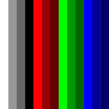
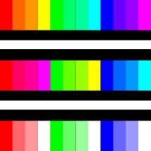
"I've never been so excited to see color bars in my life."
Project Soundbyte

Introduction
Motivation
The goal of our project is to create a VGA video adapter. This “homemade video card” should be able to connect to any monitor that subscribes to VGA standards with a standard connector and display the desired material reliably. The challenges involved here stem from adapting a general use microprocessor that we are familiar with to a specific task that it may (or may not) be suited to. The project required the researching and understanding the VGA standard of how a picture is displayed on a computer screen, identifying the shortcomings or advantages of the MEGA644 processor in accomplishing this, development and fabrication of the necessary hardware to interface with the screen, and in converting images to a format that can be stored in memory and displayed on the microprocessor.
We divided our goals for this project into a progression of three different tasks, each building off of the previous one.
- First, we wanted to display color bars on the screen, by means of direct output from the microcontroller to an analog circuit that transformed pin outs to VGA output.
- Next, we wanted to display color bars or a static image to the screen, by means of triggering RGB outputs from static random-access memory (SRAM).
- Finally, we wanted to render an animation or video to the screen, by means of triggering outputs from SRAM but also writing to SRAM live data simultaneously.
Our ultimate goal, originally, was to stream a live CCD camera to VGA output using our device. However, upon delivery of the CCD camera and studying its output, we observed very quickly that its transmitted signals were not suitable to be converted to VGA in the scope of the remaining time in our 5-week project. This will be described at greater length after a brief background about the standards and parameters relating to VGA.
While this is a “solved problem” by industry standards, it poses a number of interesting challenges to the inquiring student.
- The clock speed of the processor versus the needed clock speed of the VGA standard (overclocking).
- The onboard memory the MEGA644 has versus the needed memory (external memory).
- The exact timing needed for the VGA output standard (cycle accuracy).
- Fabrication of appropriate hardware to address shortcomings of the processor for the above tasks or in simply building hardware filters/interfaces for the VGA standard.
Research
Video Graphics Array (VGA) is a video standard devised by IBM for their PS/2 computers in 1987. The widespread adoption has since made this the baseline for all displays and is still the baseline for operation today. The standard specifies a set of screen resolutions, operating modes, and minimum hardware requirements.
There are five signals in the VGA connection that we are most interested in: two for timing conditioning and three for colorization.
For conditioning, the vertical sync pulse is a digital active low signal whose negative edge triggers the monitor moving focus to the topmost line, leftmost pixel of the screen to display RGB; the horizontal sync pulse is a digital active low signal whose negative edge triggers the monitor focus to the leftmost pixel of the next line down from where current focus is. When not in the presence of sync pulses, the monitor moves focus to the pixel to the right of existing focus, one pixel per clock cycle on a 25.175 MHz clock.
The other three signals with which we are concerned are for Red, Blue, and Green, which are each analog signals sent to the monitor. Thus, since we store values (like the colors in an image) as digital elements in the MCU, part of the hardware for such a device would require a Digital-to-Analog conversion.
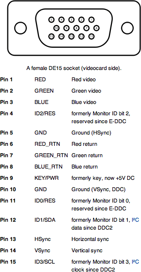
Pinout diagram of a VGA adapter, from Wikipedia
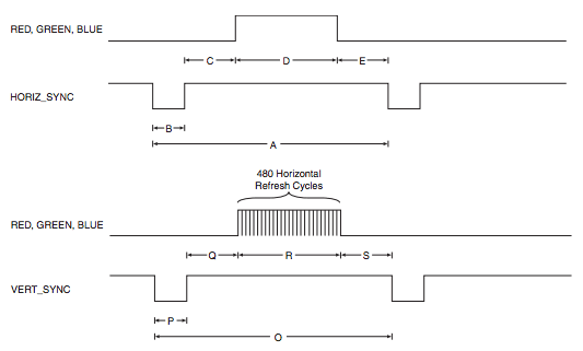
VGA Waveform Guide, from Altera
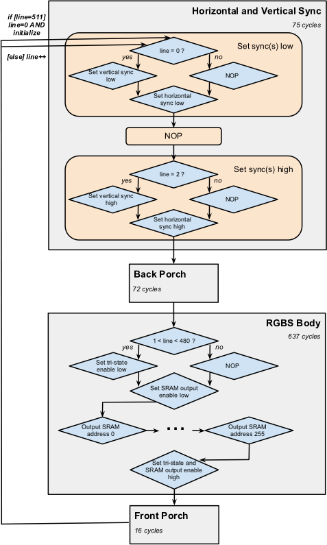
Given these five signals, we can divide each line into four distinct sections. During the first section (Vertical and Horizontal Syncs), the necessary syncs are driven low and RGB must be set to digital low, as well, for the monitor to observe the syncs correctly. To skip ahead to the third section (RGB), this is when the syncs are kept high and the RGB signals are of variable output depending on screen colorization. The two other sections (the second: Back Porch, and the fourth: Front Porch) are spare cycles that keep the syncs high and RGB low, with the direction (Back, Front) referring to the location of the porch relative to nearest sync section of relative magnitude.
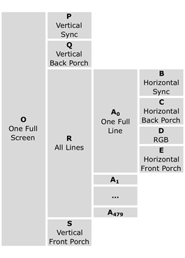
Summary of stages and stage overlap in VGA standard
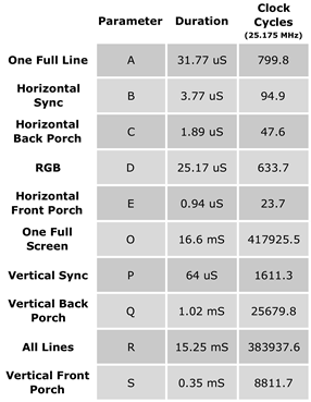
Timing of stages in VGA standard
During observation, we noticed that the porches can be used for additional computation and preparation time for the next line to be printed; however, the syncs need not be as long as shown in the diagrams above. Rather, if one wanted to, they could trigger RGB immediately following the positive edge of the horizontal sync and drive it low immediately preceding the negative edge of the horizontal sync—so as to maximize the length of color printed to the screen.
Reconsideration of Project Scope
Now, with the insight about how VGA signals and timing works, we return to the original proposal of CCD camera live display to VGA. Upon learning more about a sample WiseCom miniature camera and its limited accompanying documentation, we learned that output is a single signal consisting of sync pulses for each line and rapidly changing RGB values in between the sync pulses at a notably higher voltage. The signal appeared to be compliant with NTSC standards, which has a period of 50 uS between sync pulses (versus 31.78 uS for our VGA output).
Because of this time difference, even with implementation of a buffer and additional digital circuitry, our VGA screen could change at most once every two samples, as a result of the timing difference, making the change from NTSC to VGA functionally insignificant in terms of quality. Moreover, having to isolate the sync pulse and decode RGB values from a single signal would add to the complexity of this goal. Though possible to convert NTSC to VGA through precise edge-based interrupts, timing, sampling, and buffering, that goal seemed incredibly unlikely and also risky for the amount of time that had been remaining, and would likely have entailed in entire project in and of itself.
To replace the live camera feed as our ultimate goal for VGA display, we needed to choose another application, and, at that, one that could exhibit real time memory loading and animation during porch time. An added goal was to include user-interactivity, which would, in turn, require the use of more ports than we have availability, thus needing a design solution to address the limited number of ports.
We decided to implement a ‘Paint’-like application, to accompany the already existing Image Mode functionality, where the user loads a static images to memory. In Paint Mode, the device would take advantage of the image the user loaded previously, storing this as the background. Using a joystick, the user would then move a colored cursor around the screen, painting their choice of 16 4-bit colors superimposed on the background. In addition to allowing for user interactivity, more ports than available, and real-time updated animation functionalities, Paint Mode would require the use of multiple memory blocks, having the image stored more than once, because we need to preserve the color of the background image that is obscured by the cursor to be replaced once the cursor moves away. This added design capability would not be necessary if there did not exist a “clear” paint color that the user can select to move around the screen without painting on top of the background, thus affording an addition functionality.
Aside from working to develop a VGA driver on an MCU that is not intended to have the memory or speed to drive such a device, the most significant takeaways from this project are the understanding of VGA as a precision data vehicle and the achievement of creating a standalone and self-sufficient application to fulfill these goals. As mentioned in the initial project description, our goals, including VGA output and, now, creating Paint, are not broaching on uncharted technological territory; however, implementing these functionalities in something as low-level as assembly has the potential to offer greater optimization capabilities (and as such, reward and satisfaction at the end of the day).
High-Level Design top
System Organization
In order to meet the requirements of our final design—including display of both painted and loaded data images, we needed to implement three different programs, each executed for a different purpose.
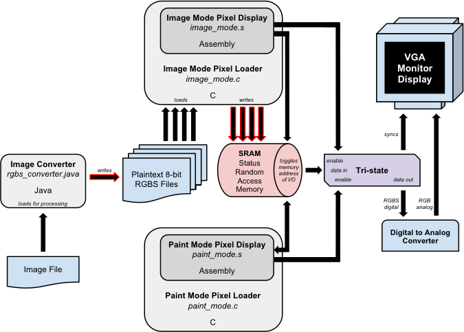
High-Level Block Diagram
Firstly, to display an image to the screen, we need to have a data point for each pixel in the image to display. We used a storage scheme of dividing our 8-bits of color data into 2-bit pairs for the colors Red, Green, Blue, and also 2-bits for shading, representing different brightness levels. For this, we created a Java application that samples, analyzes, and averages RGB data from a user-provided image for processing it into our 8-bit styled RGBS format and exported as a file.
The contents of this file can then be loaded into program memory of a second application which writes the data to SRAM, saving the pixel colors to memory for later use. After loading completes, this application displays the loaded image to the VGA monitor in 8-bit color. To display an image to the monitor at high enough of a resolution, the pixel data for the image will exceed the storage capacity of the MCU. Thus, a series of files are created for each image that is processed, which can be loaded into SRAM over the course of numerous program executions. This procedure represents Image Mode.
A separate application affords the user the functionality of the Paint Mode application described above.
On the hardware side, the necessary connections need to be made between the MCU and memory. Furthermore, MCU and SRAM output are digital, but VGA color input is analog, requiring a Digital to Analog Converter circuit. Finally, a Tri-state stands between memory and the VGA so as prevent memory’s RGBS output pins to be sending to the monitor when our sync pulses are low, so as to not interfere with pixel alignment and ruin the integrity of the signal and image.
Other important considerations and high-level design tradeoffs regarding port assignments, timing, and implementation are described in more detail below.
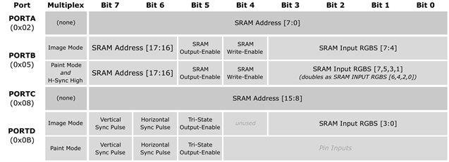
Port Assignments
Both Image Mode and Paint Mode will be displaying data from SRAM to the screen, meaning that they will each require 18 address bits as outputs (to point to a location in SRAM). Overall, SRAM has 19 address bits, but we need not use all of them. The distribution of these bits is described in more detail under the Memory Loading heading of the Software section.
Both modes also share a need to have an enable bit for the Tri-state, a Vertical sync pulse to signal the monitor for a new screen, a Horizontal sync pulse to signal the monitor for a new line, an SRAM write bit, and an SRAM output or read bit—all of which are active low.
With 23 bits occupied in each of our modes, we are left with nine to use.
In the Image Mode, it is critical that we load 8-bits of color into SRAM, allowing for 256 different colors to be sent to VGA. This leaves only one vacant port which will go unused.
In the Paint Mode, the user needs to be able to interact with the application via joystick and button, thus requiring 5 inputs and leaving 4 remaining. In order for the cursor in paint to move about the screen (and thus be written and re-written to SRAM), we need output ports from the MCU. However, in order to restore the portion of the image obscured by the cursor once it has moved, we also need to have input ports to read from SRAM.
This point represents an integral design decision in our development process where more bit functions exist than there are ports. To resolve this, we first considered the different applications of the ports in demand. Realizing that we do not have space for 8 inputs and 8 outputs for SRAM I/O RGBS data, we decided that—solely for the paint application—colorization will be reduced to 4-bits instead of 8-bits. While the Image Mode will preserve 256 colors, the paint modes pigment selections will be limited to just 16.
After this decision, we have need for 4 SRAM inputs, 4 SRAM outputs, and 5 joystick inputs (for four directions and a button), but only nine pins exist to fit these. Seeing that there are nine inputs, including two groups of four (for joystick directions and SRAM I/O), we decided to multiplex these together. Using the horizontal sync (which goes low for ~70 clock cycles per line displayed to the screen) as a multiplexing control bit, we can read the joystick inputs while the horizontal sync is low, and otherwise read the outputs of SRAM on those pins. This allows the joystick button and the outputs to write to SRAM to receive their own (un-shared or un-multiplexed) pins, unperturbed.
Output Port Assignments
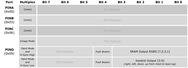
Input Pin Assignments
The final choice came to distribution of the pin assignments. The first 16 bits of SRAM address are kept together in PORTA and PORTC, so as to be easily incremented. We then wanted to put the five input pins alongside other bits that could be changed in isolation without altering them all at once (since we should not be reassigning port values for the input bits, so as to enable pull-up resistors and potentially alter our circuit conditions; meanwhile, other operations to affect a cluster of bits in a single port but not others will be more costly in terms of time, which is disadvantageous to us in this project).
Thus, the input pins were matched alongside the Horizontal and Vertical sync in addition to the Tri-state output enable—each of which is assigned as an individual bit and independently of the others—on PORTD. It was beneficial to leave the four related data RGBS outputs to SRAM I/O on another port that could be assigned as a cluster (along with the remaining two address bits, and SRAM’s write- and output-enable bits) since we note that, when looking at the library of available assembly instructions, a cycle cost of 1 is assessed for reassigning a port’s entire 8-bit value simultaneously, but a cost of 2 is assessed to alter each individual bit in isolation, making it a poor decision to have put these four data bits that are assigned to all at once alongside the input values, and instead put them on PORTB.
Timing Considerations
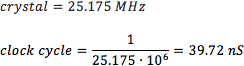
Next, we need to assess the timing of our operation. Although we generally use a 16 MHz crystal in lab, 25.175 MHz is the VGA standard, and gives us more clock cycles to work with, giving us more flexibility in operation during time that we are outputting to the display. As such, we decided to overclock the MCU by ~25% using a 25.175 MHz crystal, and, provided that, we can identify the following:
Now, we can observe how this will impact our capacity for output, knowing that we will follow the general VGA standard and spend 800 cycles processing each line at the proper frequency, and use this to identify an optimal number of lines to process to match a standard 60 Hz refresh rate as closely as possible.
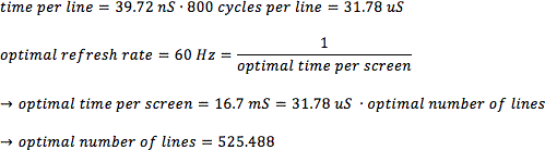
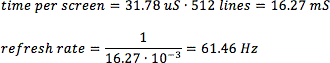
For convenience, we decided to have 512 lines per screen, and can proceed to identify the following.
Timing Tradeoffs
The most critical feature of VGA is precise and consistent timing. We observed from various examples that a single clock cycle difference between horizontal screen lines of output results in a jagged, zigzag appearance since one clock cycle difference equates to a one pixel shift.
Since each clock cycle represents a pixel, this indicates that the only way to obtain full resolution across a line is to change the output for every pixel, and thus, every clock cycle. Although our original proposal acknowledged an interest in implementing a VGA-output program in C, it became very evident through initial testing that programming in C or any other even higher level language would sacrifice our granularity over control of clock cycles, and possibly compromise consistency and precision of our output—particularly for not being able to control the compiler’s output and how many clock cycles are used for a given line of code, depending on the singular or sequence of instructions. With this in mind, we proceeded to implement the body of our code in assembly language.
Even with the body in assembly, we were left to consider different design implementations as to how to output VGA signal to the screen. Two ideas were having the assembly body output a single line to the screen versus having the assembly body output an entire screen. Having the routine called once per line means that the code needs to respond and be prepared within ~31.78 uS, but more importantly, this preparation needs to take place during the fraction of that time not being used for display (when the function can be released—less than one-fourth of that, or less than 7.9 uS). Having the routine called once per screen means that the code needs to respond and be prepared within ~16.7 mS, or the fraction of that time during which lines at the bottom of the screen are not being printed but rather withheld, which, for 32 of 512 lines would be ~1.03 mS).
These considerations were as follows:
- Executing the assembly body called from an interrupt in C
Tradeoffs: easy to implement regular interrupt; need to have a timer count to ~400,000 if implemented once per screen; losing ~70 clock cycles from entering the interrupt; losing ~10 clock cycles from entering the assembly function - Executing the assembly body called from a naked interrupt in C
Tradeoffs: more challenging to implement and preserve registers; losing ~5 clock cycles from entering the interrupt; losing ~10 clock cycles from entering the assembly function - Executing the assembly body called from an interrupt in assembly
Tradeoffs: not too challenging to implement, simply a new technique; minimal overhead; (like the above) would need to account for latency—since the processor completes the current instruction before entering an interrupt, even if it costs numerous clock cycles—so that each line of display starts at the same precise pixel; (also like the above) we would need to use caution when assigning tasks to the main routine, since we are not always guaranteed to finish them, which is arguably dangerous if the program relies on these tasks completing to re-write part of the pixels in memory before the next screen - Executing the assembly body in an assembly loop
Tradeoffs: the most intuitive to implement; most granular control over allocation of cycles; least associated overhead; requires the rest of the application to be programmed in assembly; requires the most time to construct, debug, and track memory, register assignments, cycle accuracy, and other low-level parameters that are generally taken care of in higher-level languages
In the interests of pushing the capacity of the MCU as far as possible, we began testing concept [1] just to see if it would work. We could observe that the output was consistent and the interrupt was being called in equal intervals in trials with a prescaler of 1024. However, as the prescaler was lowered to approach the realistic and required value of one, we noticed significant performance degradation and lag time on interrupt calls, eliminating this from our list of viable solutions.
We proceeded to investigate naked interrupts for concept [2], and began conducting trials with those but noticed performance degradation here, as well, although it took longer to reach lag here than in the previous case, but it still occurred before reaching a prescaler of one.
Between remaining concepts [3] and [4], we decided in the interests of granular control to pursue concept [4] since we would consistently be fully cognizant of the number of clock cycles for performance and could use that insight to keep our options open for project extensions and a larger pool of potential applications to display on the VGA later in the process once image display was successfully achieved.
Hardware top
Schematics of the displayed circuity available in the Appendix.
Hardware Selection
The necessary considerations for the selection of the hardware were driven by the need to execute tasks that the microprocessor that we had the most familiarity with [the Atmel MEGA 644] is not particularly suited for the task of driving video. While not totally impossible, a professional hardware designer would make different architecture choices to leverage innate capabilities of different processors and their I/O configurations. We saw this as a primary challenge to the project and set about initially to improve upon other examples in terms of screen resolution and execution features.
The initial hardware platform was inspired through a reference project where someone attempted to build a VGA driver using the 644. The basic platform was adapted to our needs and then added ot as necessary to confront the hacks others used to overcome the system limitations.
The basic task is to write pixels to a screen. Considering the VGA standard of 640 x 480 active pixels, this yields over 300,000 pixels sent to the screen 60 times per second. Each pixel can be represented as a byte to yield a 256 color palette, and this in turn, generates 2.45 gigabits of information to output to the screen at 60 Hz! Needless to say, this is far beyond the memory capability of the MEGA 644, even if were to co-opt all of the EEPROM, which is only good for 2KB. Therefore some serious outboard memory will be required.
Additionally, the flow control of this data stream needs to be tightly controlled and data bus collisions must be avoided for this to work. Therefore, a traffic cop is needed to enforce blanking intervals to ensure proper synchronization and to allow for writing information to the outboard memory as well as reading the stored memory to send it to the screen. For this we will use an Octal Bus Transceiver (here after referred to as a ‘tristate’) because it has the attractive features of enabling through 1-bit control and effectively prevents reverse biasing, an important consideration which will be revisited later in the project.
The last component of the core hardware is a DAC to interpret the color palette we have sent to the screen and generate the analog R-G-B information that the VGA monitor is waiting for. While DAC’s are available, a simple passive component DAC was chosen for several reasons most important of which is that it works well.
With these needs in mind we confirmed our use of the MEGA644 and selected a 512 x 8 Static RAM chip, a LS74245 octal bus Transceiver, and used lab surplus resistors and diodes to build the analog DAC. The choices of the hardware reflect the concept that we will be dealing with the data a byte at a time and do not need bit-accurate recall; one command reads, writes or passes through a byte (colored pixel) in one motion. Given that the response time of the SRAM is on the order of 10 nS, this will be quick enough to work; older hardware such as the eeprom chips kicking around our shop have both insufficient capacity and their access times were too long by at least an order of magnitude.
The real difficulty in the SRAM concept was the package. Chips of the capacity and speed to fit our needs are not available in a PDIP format. I saw a number of ‘creative solutions’ to this problem on hobby websites and came up with the idea of soldering ribbon cables to the j-pins of the SOJ chip we had and terminating them to a 40-pin IC socket. (It seems that a 36-pin adapter either does not exist or is sufficiently rare as to avoid detection.)
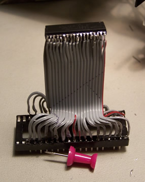
SOJ SRAM Conversion
Next, the logic gate array that will interface with the processor was built using standard LS-series logic linear circuits; these are industry standard and even if our processing time is fast, the switching characteristics of these common chips are generally fast enough: on the order of 8-15 nS.
The last selection was to be that which drove the entire project: the timing crystal. The AT MEGA 644 is rated to run at 20 MHz, however the VGA standard is 25.175 MHz. This would mean ‘overclocking’ by almost 29%. Overclocking results in higher power draw, higher operating temperatures, and the possibility of processor breakdown through timer errors or the inability of outport ports to cycle fast enough. Obviously, we took the overclock route and selected a 25.275 MHz oscillator crystal.
Power was supplied by a standard 7805-style voltage regulator, a 340T5. This supplies a regulated 5VDC supply at 1.0 A (more than enough!) and we added 2 bolt-on heat sinks to accomplish sufficient dissipation. The circuits were assembled on spare solderboards found in the MAE and ECE labs that had friendly configurations and were populated by hand.
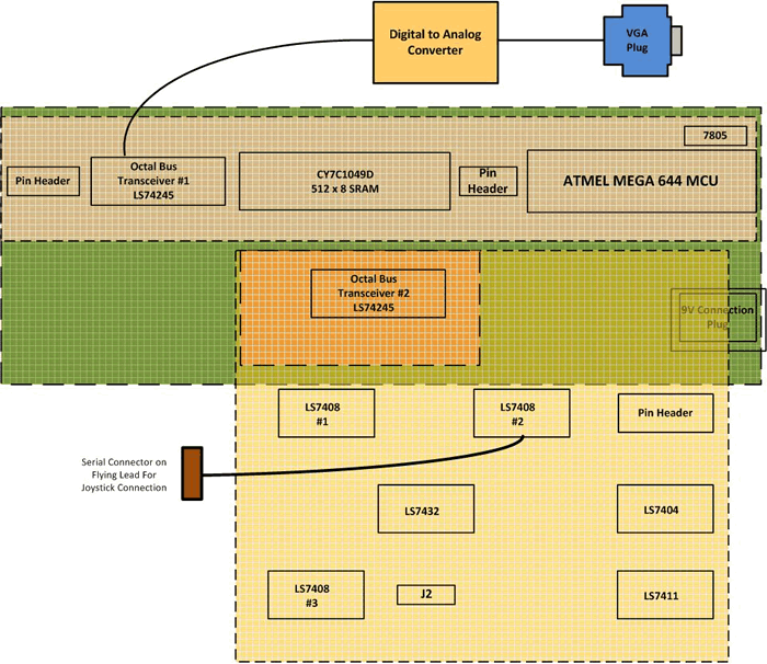
Hardware Layout
Signal Flow
Signal flow is generally not as one would expect, that is that the MCU would access the byte stored in memory and send it to the screen. Not only could the processor run fast enough to accomplish this, but there is no real need to do so. Rather, the MCU sends a stream of addresses to the SRAM, which then dumps the needed byte directly to the tristate to be exported to the screen.
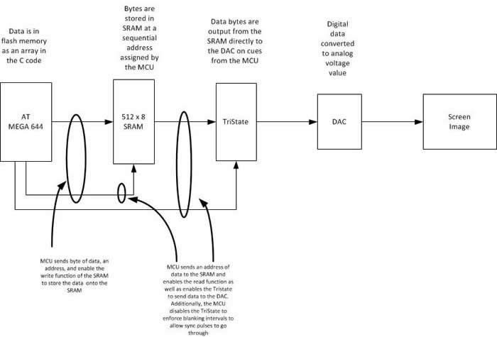
Image Mode Hardware Flow, write information to SRAM and display a static image
In the Paint Mode, the image needs to be updated by some method and then sent to the screen, thus requiring the additional steps of updating the pixel information and writing the byte to the SRAM so that it may be sent to the screen in the future. The block diagram would look the same; the MCU would simply add the process of repeatedly iterating the write process as well as the read process of the SRAM. This would affect an animation or a trace being drawn across the screen, for example.
If a user interface is desired, then the flow is more complex with the selection of enabling the signal from the user (such as a joystick) when there is no signal being sent to the screen.
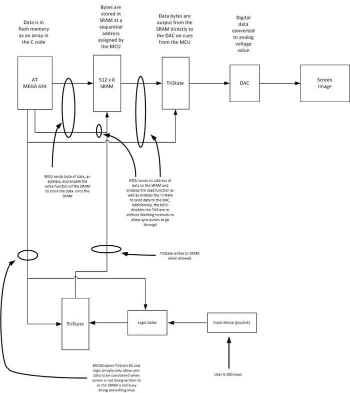
Paint Mode Hardware Flow, interact with user input
Logical Design
The purpose of the logic gates is to enable/disable data flow based on the state of the MCU and therefore the SRAM. We could have done this through a separate pinout from the MCU, unfortunately, the ports are fully populated and so we required a passive method of doing this.
The logic gates are also buffered by the TriState #2, as previously mentioned. If this was not done and simple And gates were used, then when the user signal was disallowed the output would be driven to a logical low and data collisions would occur. Moreover, by using a truth-table style approach to scheduling of user interface we were able to exploit those valuable times when the processor was not parsing data to the screen to interact with the user or to process the image itself.
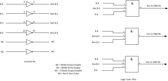
Logical Enabling of User Interface
Final Architecture
Our final hardware architecture evolved into something quite different than what it started as due to the limitations of the microprocessor and the desire for enhanced functionality. In order for us to be able to implement a paint-style application it became necessary to create additional functionality independent of the MEGA 644. Additionally, we used a set of manual jumpers and multipin headers to switch between operational modes.
For example Jumper J1 selects which half of the SRAM’s memory addresses are accessed by manually setting the Most Significant Bit to 1 or 0. We were simply out of Pins on the 644 to access all the addresses any other way. Likewise, Jumper J2 selects or deselects the logic set depending on which operating mode you are using, much like any number of computer components such as hard drives.
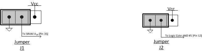
Mode Selection Jumpers
In similar fashion we access the I/O ports from the SRAM differently depending on whether we are programming to a 256-color palette or drawing using a 4-bit color choice. This low-tech solution to a high-tech limitation is a great way to leverage your resources when needed.
Lastly, it should be observed that we now understand completely why today’s modern video cards are so resource-intensive or resort to using system memory to render viable graphics. In order to render VGA-standard resolution with a reduced color palette, we overdrove our little microcontroller to a ‘screaming’ 25.175 MHz and loaded up just over 4MB of external memory; todays video cards often exceed 3 GB of memory and utilize processor speeds exceeding 3 GHz in order to drive a modern high resolution monitor with the millions of colors we demand….and they have no part in the implementation of the application that they are displaying!
Software top
Image Processing
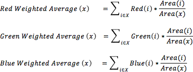
One of the component functionalities of our product allows users to display their own image on the VGA monitor. In order to resolve the provided image of variable input resolution to 256 x 480 (shown on a 512 x 480 canvas), a Java application retrieves the input image and divides it into 122,880 (or 256*480) equally sized rectangles, each taking up 1/255 of horizontal space and 1/480 of vertical space.
For each rectangle in the prospective newly-resolved image, the program reviews all pixels in the input image that lie within that rectangular space and collect their RGB values. Then, it will compute Red, Green, and Blue values for the rectangle by summing the Red, Green, and Blue values of the pixels in the input image that lie within that rectangular space, weighting each value by the fractional area the given pixel inhabits in the area of the whole rectangle whose RGB is being identified.
This weighted average (for each Red, Green, and Blue) is between 0 and 255, and is calculated using the formula below where: x represents a pixel in the newly-resolved image, i represents a pixel in user’s provided image, and X represents the subset of all pixels i that are contained in rectangle x when the new and old images are scaled to be of equal dimensions and superimposed.
For our 8-bit colors, we assign two bits for Red, two bits for Blue, two bits for Green, and two bits for Shading (which makes the displayed color brighter or more white-based, which we will return to later). Thus, we needed to map the domain of 0 to 255 to the range of 0 to 3 for each color. For the entirety of the domain 0 to 255, the goal is to identify a function that has each of the output values (0 to 3) evenly represented. We do this keeping in mind that for the paint mode of the application, values will re-be colorized from 8-bit to 4-bit; since the most significant bit of each color element (RGBS) will be used independently for that conversion, we want to ensure that having the color asserted or not asserted happens for an equal range of our 8-bit or the standard original image's 8-byte input domain. For this, we can right-shift the RGB values by six to reduce the initial 8-bit value to a 2-bit one, also maintaining evenness of domain distribution across the range.
Finally, we calculate the shading—with higher shading values indicative of more brightness. For this, we surveyed 8-byte colors to qualitatively observe trends that dictate noticeable brightness changes. Namely, we saw that increasing the Red, Green, or Blue in isolation (with the others set to zero) results in—obviously—increasing the presence of the color, but lacks a noticeable change in brightness, even when the changing color has been adjusted to 255. As such, the mapping function that we use to determine the two shading bits from RGB will likely not include R, G, or B values by themselves in a sum. Rather, increasing a pairwise combination of Red, Green, or Blue results in noticeable brightness changes.
Thus, we can calculate a shading score as follows, where WA stands for the weighted average from above, and x represents the position of a pixel in our newly-resolved image:

We continue using the weighted averages since they offer more control over granularity for our calculations. Next, we analyzed greyscale colors (where Red = Green = Blue exactly) to look for the qualitative point at which brightness levels change dramatically. We selected 190, 210, and 230 as those points, and solved the above equation for Shading with those as input parameters. Thus, if a given pixel in the newly-resolved image maps to a Shading(x) below that of the first threshold (190), shading is zero. For values above 190's shading but below 210's, shading is set to one; above 210's but below 230's, shading is two; and above 230's, shading is three.
Memory Loading
First, we needed to determine how to assign the 19-bits address bits of SRAM so as to store pixel information. 8-bits were assigned to represent the x-component of the pixel position on the screen (which does, in fact, range from 0 to 255). 9-bits were assigned to represent the y-component of the pixel position (since these range from 0 to 480, where 512 is the lowest power of two to contain them); furthermore, we actually write 512 lines to the screen (although the bottom-most 32 lines are empty and only used for processing and memory-interaction time), this simplifies things. There are two unused bits, indicating that our 512 kb SRAM can store four images in all. For the purposes of our paint application, we can toggle between two images using bit 17, controlled by the program. Bit 18 is left as a manual switch that the user can toggle to choose the half of memory that they want displayed (or which two-image storage cluster, high or low).
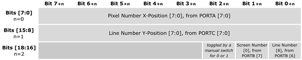
Assignment of SRAM Address Bits
Now that the algorithm is complete, the Java program requests the user to input a file path for analysis, and then asks the user for a path to write a collection of files containing a snippet of C source code to be included—holding an array declaration of byte values to be stored for part of the image. Program memory offers a storage space of 65,536 bytes. For our 256 x 480 resolution (displayed in a 512 x 480 frame), a still image occupies 122,880 bytes of memory. The entirety of the screen (which will require eight defining bits for the address’ x-component and nine defining bits for the address’ y-component) will occupy a space in memory of size 256 x 512, or 131,072 bytes, ignoring unused lines at the bottom—exactly twice the size of the program memory capacity with no extra space. As such, we decided that it was best to write to SRAM a minimum of three times.
Furthermore, arrays in C cannot occupy more than 32,767 bytes, so since each of the elements of our array is a byte, the largest number of entities that can be stored in the array is 32,767 (or one less than 2^15). For simplicity and convenience, we have devised a scheme that writes to SRAM four separate times; each time, we write the values stored in an array of maximum length to 32,767 addresses in SRAM (losing one pixel at the end, but avoiding visual incongruities by hiding the last column of each line when displayed on the screen so that a crisp line exists at the right-side of the image). Bits 17 and 16 are held constant for each program execution. As such, the Java program outputs four files, each containing an array of length 32,767 where the value is the 8-bit RGBS value and the index represents the 15 least-significant address bits. Accompanying the array is another variable, representing the two most-significant address bits for the partner array.
Alternative solutions could have carried out in only two or three program memory writes to SRAM; however, these solutions would have sacrificed code readability, intuitiveness, ease-of-use, and convenience when a single program execution is capable of adjusting any combination of the 17 address bits that we are using, instead of keeping the two uppermost constant and the others gradually incremented. This was a design tradeoff with which we were satisfied. Moreover, we opted to continue using a single array for each memory load for much of the same reasons. Even with multiple arrays, we could not increase the memory load of a single program execution by a single power of two over the existing implementation, more so discouraging deviation from the existing design as there is not much to stand to gain as a result.
Image Mode
The first mode in which our VGA adapter can be used is to load and display static images to the screen. Since the precision of the loading component of this mode need not be cycle-sensitive like sending images to the screen, we can implement this in C. Then, as discussed earlier, actually sending the SRAM data to VGA is implemented in cycle-accurate assembly.
The procedure for the C routine is relatively simple.
We take the code snippet from our image processor and include it in variable declarations storing the array in program memory. When the program begins to execute, we stall for a milliseconds to allow SRAM to initialize, so as to not blow the internal transistors in the chip and render it non-functional. Then, we iterate over the elements of the array, output the value to the I/O ports of SRAM, and output the address of the value to the SRAM address ports.
Once this is complete, we can briefly set the SRAM Write-Enable to low to write the value to memory while keeping the other active low enable pins at a logical high (including the SRAM Output Enable, Tri-state enable, and Vertical sync pulse). The Horizontal sync pulse is kept low for reasons of multiplexing the versatile pins on the microcontroller that serve multiple purposes at different times or in different modes; however, this has no impact on the output since the Tri-state enable is kept high, preventing signals from being transmitted to the monitor.
As mentioned before, the fifteen least-significant bits of the pixel’s SRAM address are determined by the index of the array value while the two next-least-significant bits are defined for all values in a particular load file code snippet. Meanwhile, the most significant bit is set manually. Generally speaking: enable, write-enable, and read-enable pins are kept on for a few clock cycles to allow for the estimated logic propagation to take place in the breadboarded digital circuits such that the signals reach their destination before enable bits (as potential multiplexing bits) are disabled once again.
Upon completion, we proceed to the display stage.
Based on our earlier calculations, it is essential to be cycle accurate, regardless of what branches are being executed throughout the program: the RGBS must start and end at the same exact same time and pixel, every time. Knowing this, each required operation was recorded, and the total number of clock cycles throughout the program was managed to ensure cycle accuracy.
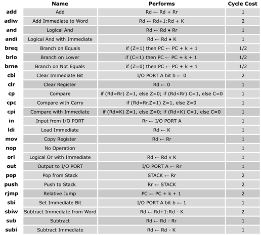
Summary of AVR Assembly Instruction Set, from Atmel
In the display mode, using a loop, we assert the vertical sync as low to begin a screen, the horizontal sync as low to begin a line, and enable Tri-state and SRAM output to send 8-bit RGBS values to the DAC for processing and to the monitor for display. During RGB display time, it will always cost us one clock cycle to increment the memory address and another clock cycle to output it; thus, in our current implementation, the best performance that we can maintain with a reliance on external memory is having each splotch of color last for two clock cycles and, as such, two pixels horizontally. Other considerations for improving or expounding upon this issue are addressed later in our Results.
Program Flow of Image Mode
Paint Mode
The second mode in which our VGA adapter can be used includes a ‘Paint’-like application. The user can start with a blank screen or an image already having been loaded into SRAM and then draw on top of the image in 4-bit colors—where one bit is used to represent each Red, Green, Blue, and Shading.
From the user perspective, their interactions with the application abide by the following usability requirements:
- See the image already loaded in SRAM with 16-bit color displayed to the screen. (A)
- See a cursor (a square, serving as your paint brush) displayed on the screen, having a write border outside and your selected paint color inside. (B)
- Press a button to toggle the color of your brush between 16 different 4-bit color options. (C)
- Draw in the selected color on top of the image as your cursor moves about the screen. (D)
- Have the ability to select a “clear” or null color so as to not draw on the image as your cursor moves about the screen. (Since we have the shading bit, binary 1111 and 0111 will appear the same, so we can have one of these serve as white pigment and the other serve as clear.) (E)
Fulfillment of this application included the following operational requirements, derived from the above user-display interactions:
- Draw the image stored in SRAM to VGA. (a)
- Allow the user cursor to move about the screen, storing last movement. (b1)
- Superimpose the user cursor on top of the image. (b2)
- Read joystick directional input to determine cursor movement. (b3)
- Return pixel contents to their original form after cursor has moved away. (b4)
- Read and debounce the button to determine pigment changes. (c)
- Superimpose the selected pigment color on top of the center of the cursor. (d1)
- Store permanent changes to the screen from painting non-clear colors. (d2)
- Disable permanent pigment changes when selected color is clear. (e)
Given the timing constraints, one of the most taxing elements of the project was developing an entire program flow in assembly. Trying to be clock cycle conservative, we worked to maximize available register space by intelligently determining the most necessary and important values to be stored there.
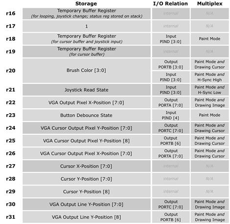
Register Assignments in Paint Mode
In order to accomplish prongs [b2] and [b4] specifically, we realized that we needed to store two copies of the image in memory, since we will recover the bits obscured by the cursor once the user migrates the cursor somewhere else. This is necessary since our time constraints will not afford checking and branching on cursor location while signaling memory addresses to be sent to the Tri-state. Knowing that we have enough space in SRAM and address bits on the port of the MCU, we noted that we could store the entire image in two locations in memory. Although bit 18 is manually toggled, the program has control over bit 17 and as of yet has no use for it. As such, for duplicate images stored in contiguous memory blocks sharing the same bit 18, we can store the foreground image (or what SRAM outputs to the display) in the slots where bit 17 is ‘0’. In the slots where bit 17 is ‘1’, we can store the background image, or the image with permanent paint pigments but not including the cursor.
As such, between each screen print, we can recover the pixels from ‘SRAM[17]=1’ elements where the cursor is covering it in ‘SRAM[17]=0’, write any pigment changes from a moving, non-colorless cursor to the background image in ‘SRAM[17]=1’, and then re-draw the cursor on top of the foreground image.
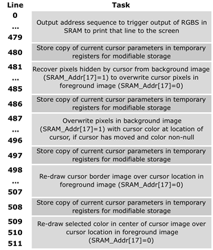
Tasks by Line Number in Paint Mode
In regards to inputs, we sample the joystick directions approximately thirty times per second, as a balanced speed for the user to move the cursor that is neither too fast nor too slow. Although the directions need no further transformation, the button that is pressed to adjust paint pigment color does need to be debounced to prevent the user from toggling through multiple colors unexpectedly from a single button press.
The following state machine for the button debounce executes only during the time at which the horizontal sync pulse is drawn low and only while line 486 of the screen being displayed (after RGB has finished being sent, but the program is polling user input for cursor movement before printing the cursor once again to the foreground).
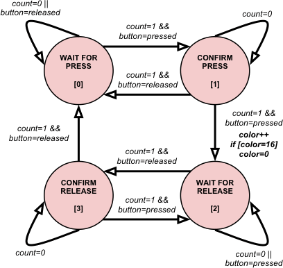
Debounce State Machine for Color Toggle Button
Using this bottom-up approach, we can combine the individual components explained above to create a script to execute Paint Mode on the associated hardware, which can be diagrammatically explained as follows, including clock cycle distribution and equality.
Program Flow of Paint Mode
Results top

Original JPEG
256-Color VGA Bitmap
VGA Standard
We started testing without SRAM or many other circuit elements, but instead, simply sending static colors to the screen directly from the MCU without any intermediate stops. This allowed us to better understand the timing constraints of VGA. Oddly enough, in spite of ample documentation for VGA timing standards, our testing revealed that many of the listed timing requirements are not heavily enforced by the inherent technology. For example, new lines were triggered by the negative edge of the horizontal sync pulse, but the duration of the pulse was irrelevant. Further, the cycles within the porches could also be moved about wherever necessary, and if need be, RGB could begin transmitting immediately before or after the horizontal sync is low. The only constraint that was observed to be detrimental to the display operating correctly was asserting RGB when sync pulses are low.
As such, we adjusted most of the timings in our routines based on logical order and flow, and maintaining RGB sent to the monitor for as long a time and as long a line as necessary, observing that no quality loss existed by deviating from the published times. Even the number of clock cycles between sync pulses is unrestricted (though resulting in a different refresh rate); however, varying the number of cycles between syncs amongst lines in close proximity leads to a jaggedness in the display, and depending on the delay, potentially even a static discontinuity across the full length of the horizontal.
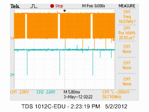
Before continuing, we used the oscilloscope to confirm that the system was behaving as expected. Namely, RGB outputs should consistently be held to zero when the Tri-state is disabled, and the Tri-state should be consistently disabled when either of the syncs are low.
CH1 Horizontal Sync, CH2 Tri-state Enable
The horizontal sync goes low once every 31.78 uS, once every 800 clock cycles. The Tri-state is only enabled to transmit RGB when the sync is not low.
CH1 Horizontal Sync, CH2 RGB
RGB is never asserted when sync active low.
CH1 Tri-State Enable, CH2 Vertical Sync
The vertical sync goes low once every 16.27 mS, once every 800*512 clock cycles. The Tri-state is disabled during lines 480-512 and 1-2 for vertical sync time.
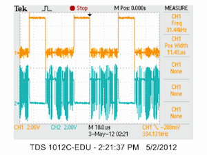
CH1 Tri-State Enable, CH2 RGB
RGB is only asserted when Tri-state enabled low.
Integrating SRAM
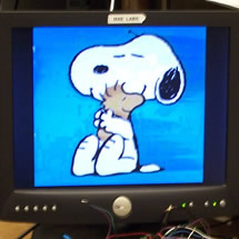
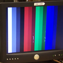
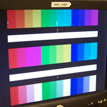
We then proceeded to connect SRAM and send values stored in memory to the Tri-state, DAC, and monitor. We started with color bars (greyscale, monochrome, and multi-colored) to confirm that the analog component was wired correctly and the order of the bits was as expected. After this, we advanced to basic pictures, whose conversions to a 256-Color scheme is less lossy than photographs.
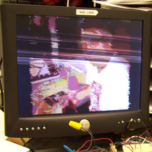
As expected, photographs do not convert as well to our 256-Color scheme as drawings or images created with a quantized palette of basic colors do. However, some photos convert better than others. The most lossy range seems to be that of mid-level, semi-bright colors, including some kin tones, indicating that we could return to our algorithm for calculating shading and consider raising the thresholds required for shading bits to be asserted.
One observation of note is the consistency of SRAM. After power cycling, the contents of SRAM are cleared, and the display appears like static, indicating a variety of numbers near to or around 255. When we first began using SRAM, it was extremely reliable and consistently output what we had written to it. However, we noticed after significant amounts of testing that some bits, often random, would get overwritten by static upon further compiles. Since we load an image to memory over the course of four compilations, we noticed that the most recent load was always preserved; however, as later loads took place (even if consecutive loads and compiles were of identical code) a few new pixels would get drowned in static. We attribute this to the rapid frequency with which we are interacting with the chip, and perhaps unreliability between the SRAM to Tri-state connection.

Port Interference
Without a tri-state or other barrier between the pins that write to SRAM during the memory load stage, this connection remains intact during the time that the MCU calls the SRAM to output to the Tri-state and display to the screen. When we forced those outputs low, we observed a generally black screen with few consistent splotches of color and far between. Forcing those outputs high observed a similar result, but white-based. Turning the MCU outputs into inputs with high impedance during the display stage resulted in jagged lines indicative of inconsistent timing across the screen, and generally one of more drastic discontinuities, as can be seen on the left below. Adding a pull-up resistor pacified the drastic discontinuity but left many of the smaller ones intact.
The only way for the image to appear with crisp borders and lines is to remove the connection between those ports and SRAM entirely during the display stage, as seen to the right. This seemed to indicate that even when a port was not asserting any voltage, simply being a connected input causes the monitor to receive the RGB signals late, yielding a jagged edge and sometimes even static. Although we speculate that the cause of this may be processor delay, since the processor directly outputs the sync functions and thus must be lagged from the changing input voltages, or even line delay, we have not been able to confirm the source.
Ports Connected as High Impedance Inputs
MCU's Ports to SRAM I/O Disconnected
Possible Extensions
One of our previous goals that is worth future consideration is achieving full resolution with a MEGA644. We settled for half resolution, since it takes one cycle to increment your address counter and a second cycle to output it, meaning that we can trigger a new pixel at most once every two cycles in this configuration. One possible solution is to clock the crystal at twice VGA standard, or 50.35 MHz, thus executing two instructions in the time that the monitor has shifted focus by a single pixel. Alternatively, one could use double buffered memory with dual processors running concurrently, alternating frames, and synchronized via SPI.
Additionally, if we conduct a brief analysis on the final version of the Paint Mode procedure, we can observe that there are at least 100 free cycles per line that can be used for computation. Furthermore, the operations taking place between line 480 and line 511 can easily be consolidated, seeing as how the cost of many of them is only on the order of tens of cycles rather than hundreds. The current implementation was devised this way nonetheless for readability and debug-ability, but further, since the scope of this project did not have any additional computation to take place, thus not sacrificing anything for the convenience of that design decision. Leveraging these otherwise unused cycles for addition lines or columns, barring memory issues, is certainly possible under this configuration.
Another alternative that was not brought to our attention until the final few days of the project is the possibility of using a MEGA128 instead of a MEGA644, so as to allot for more ports, easing the need for digital logic and simplifying the design.
Conclusions top
Meeting Expectations
Our final design was able to successfully read from and write to SRAM and trigger SRAM addresses to output stored data through the Tri-state and DAC to produce a crisp image of user choice on the display. In terms of usability, our design was satisfactory. The issue with having so many different stages and programs in the design, as a result of circumventing memory restrictions, is that the operator must be familiar with the procedure for the system, and as such, it is accompanied with detailed instructions from the very first step when the user submits an image for processing. The device has not realized any safety flaws, and has no accuracy measure except for the similarity or dissimilarity of submitted images to their on-screen 256-color counterparts. We believe that the device performs well in this capacity, and can further improve as more complexity is added to the 2-bit shading calculation. For interference, we have recognized and sidestepped and issue with port conflicts resulting in static and delays affecting the screen impression. Finally, speed of execution is a regime in which our design reigns superior, having been coded in assembly language for cycle-accurate, optimum performance. Although the speed of the design cannot be improved upon without changing the screen refresh rate, we could, in the future, seek to add or consolidate more computation during the time of processing.
From a personal standpoint, I (Ryan) recognized midway through the design process that our project, originally intended as a simple pursuit to better understand and optimize image displays with an MCU, inadvertently ended up being the perfect capstone to my undergraduate career in ECE, embracing a healthy balance of the broad majority of core classes in the department—ranging from manipulating voltage signals, to design of analog circuits for RGBS output, digital logic for toggling between assignments for our limited number of ports using multiplexers, extensive assembly programming, memory distribution, and knowledge of embedded computing.
Having reached the close of the project, we developed a working product that fulfilled both the letter and the spirit of the project requirements, in the sense that our VGA adapter and application was built around and fully utilized the functionality of the microcontroller. Instead of using the microcontroller for data collection and implementing the display and processing functionalities in a more high-level coding language and with use of a software package, one of the big takeaways here was the satisfaction of having developed a functional product and video driver that executes in isolation, without reliance on external libraries (with the exception of accessing memory in PROGMEM). Furthermore, to go a step further, much of the code involved exists at the basic level of assembly, demonstrating ability and throughput to create, manage, and execute an advanced, time-sensitive design on a very low-level. As such, the scope of this design does more to demonstrate understanding and use of the microcontroller and time-sensitivity than it would be having used it for data collection alone and allocating heavier processing elsewhere.
Societal Impact
There are many applications where the human interface to a microprocessor is integral to the functionality of a task, yet it is often the case that those same interfaces are woefully inadequate past the point of debugging or demonstration of concept. Input devices such as button or keypad presses or even keyboard-and-mouse entries are generally sufficient both from a usability standpoint and from adequacy of the type of information gathered without being excessively onerous to accommodate programming-wise. It is the output however, that is often lacking in clarity.
An LCD screen is quite inexpensive and easy to set up, but you are restricted to small set of characters (mostly alphanumeric) displayed in monochrome dot-matrix style. It does not even execute quickly. While these shortcomings don’t really matter with a simple information stream, such as a reaction timer high score, anything of more complexity is all but lost. The situation improves with a serial communication tool such as Putty or the once-ubiquitous HyperTerminal in that strings, numbers and the like may be sent to a screen with improved flexibility and speed. A graph can be created using ingenuity in placing symbols on the page like dot-matrix printers of the 1970’s did, but that is where the capability ends; a picture is out of the question.
Suppose you wanted to display a photo taken by a robot’s on-board camera. Or perhaps you wish to display the results or condition of the process in question in a truly intelligible fashion. The successful execution of this project and further extension for data transmission and storage can allow for all of that and more. With this system, it would be possible to output full VGA images to nearly any screen available with obvious application to demonstrations in labs or views of working equipment and processes with the interface being made by an $8 chip.
Standards
The standards relevant to this project are fairly straightforward in that the goal is based around being able to get the microprocessor to output a signal that adheres to the VGA Format. Quite obviously the most important standard is that of the Video Graphics Array by IBM which specifies a set of screen resolutions, operating modes, and minimum hardware requirements. Additionally, VGA spells out voltage, impedance, refresh rates and color palettes; NTSC-M dictates color coding. Other standards that have an influence on the parameters of the project albeit tangentially are those referring to VGA configurations [IEEE 1275-1994], SRAM [JEDEC 100B.01, JESD21-C], and microprocessors themselves [ISP 35.160].
Safety Considerations
As with any application using consumer electronics, especially when one is intentionally hacking in to a system, there exists the risk of electrical shock. Fortunately, all of our work was constrained to the low-voltage side of the equipment. All of the voltages that we were dealing with were 5VDC or below, thus effectively removing that danger.
The use of soldering equipment carries with it the obvious burn hazards as well as the not-so-obvious hazard of lead exposure from the solder and smoke as the better solders do indeed contain lead. This was mitigated by frequent hand-washing , especially before eating and in a conscious effort to inhale as little smoke as possible when soldering in well-ventilated areas.
Lastly would be the risk of fire that can arise from electronics, especially those being driven above their ratings. While our setup did indeed get quite hot at times it was never left unattended or in the immediate proximity of combustible materials.
Intellectual Property Considerations
The VGA standard was implemented in the 1987; it is still the default minimum standard to which all computers must adhere. As it is a standard, and an old one at that it is to be adhered to rather than patented.
The hardware we used was all off-the-shelf grade material and no proprietary software was used. Circuit designs were all standard practice methods and (as stated in the Hardware Development section) the initial core hardware layout was inspired by tutorials on Lucid Science . References on software techniques and the like were all openly published and their use was encouraged. Nonetheless, all computer source code was original with the obvious exception of C libraries used by the Atmel Compiler.
We are not seeking a patent or any other exclusivity for any part of his project; this was done as an investigation of a ‘solved problem’ in order to further our understanding of the use of microcontrollers.
Acknowledgements
We would like to thank Bruce Land and the Spring 2012 ECE 4760 TAs for their ideas, insight, and dedication. In many cases, their advice from experience and suggestions from domain knowledge saved us hours of potential mistakes, component seeking, debugging, and deliberating, and as a result, their efforts contributed greatly to our project's success. Moreover, their commitment to the course and countless hours in lab and lecture not only worked to improve the quality of our final product, but furthermore, improved the overall quality of the design experience from taking this course. Much gratitude goes out to all those involved for using this course as a forum to instill passion and excitement for engineering design.
Appendices top
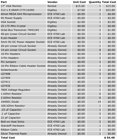
Parts List
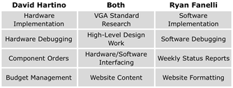
Task Distribution
Schematics
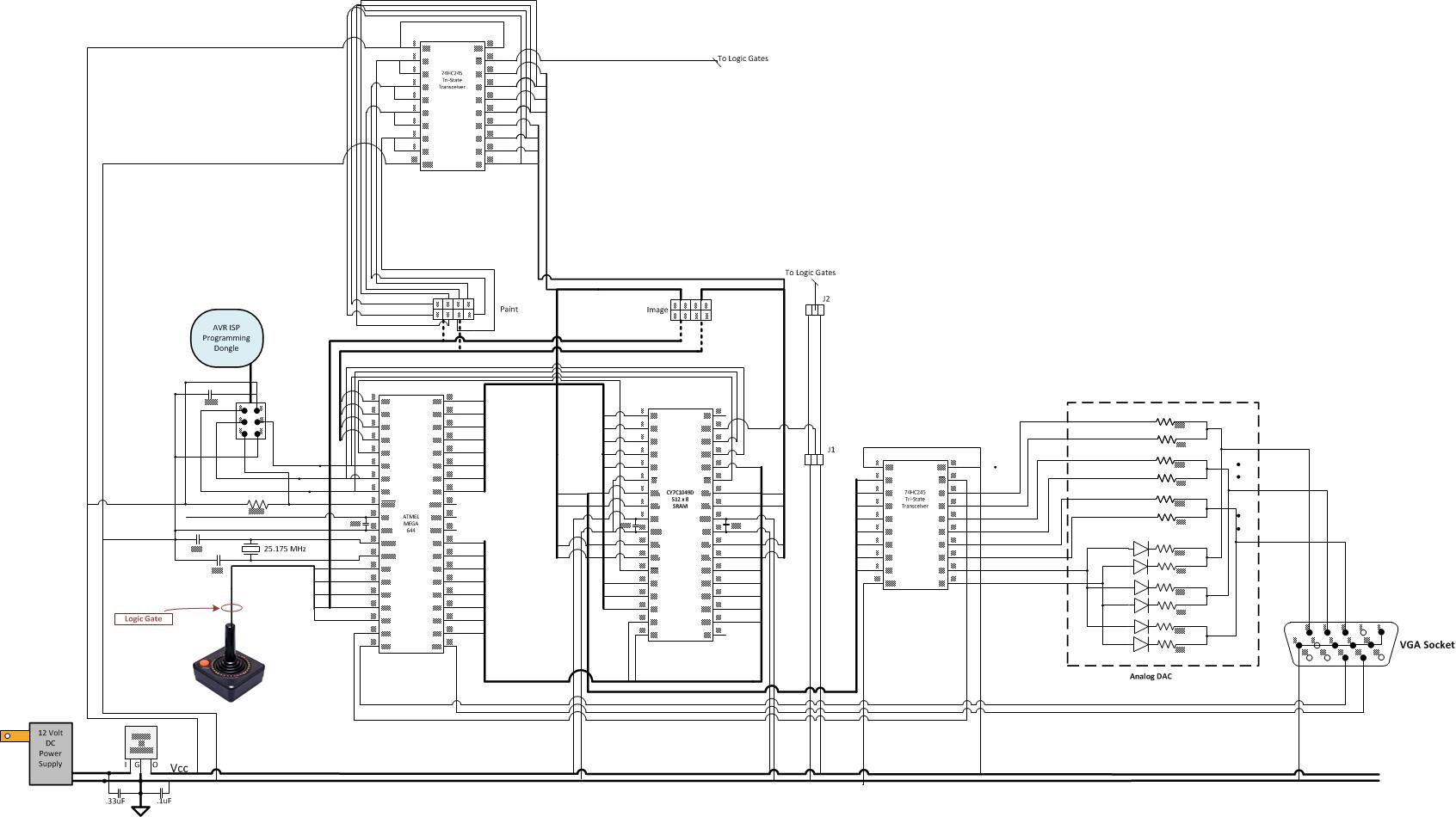
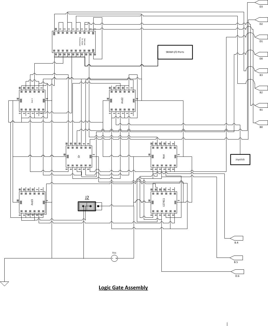
Code
- Image Converter (rgbs_converter.java)
- Sample Images and Output (rgbs_examples.zip)
- Image Mode Data Loader (image_mode.c)
- Image Mode Pixel Display (image_mode.s)
- Paint Mode Program Loader (paint_mode.c)
- Paint Mode Pixel Display (paint_mode.s)