Introduction top
This project aims to implement an efficient fractal calculation engine (Mandelbrot Set), and manipulate the color rendering process in real-time based on the FFT analysis of input audio. The mandelbrot set is displayed via VGA port with High Definition Resolution (1024x768), and user can either move or zoom the display via sending simple command through UART (auto-baud) or pressing specific control keys on Remote IR Controller. To realize color manipulation, a color palette is implemented as a dual port RAM which allows modificaltion in real-time. We then map the FFT audio analysis result to mandelbrot set's color rendering space. By doing this, the color of mandelbrot set will change as the audio data flows in. The whole system block diagram is shown in Figure 1. The hardware paltform used in this project is DE2-115 board with Altera Cyclone IV (EP4CE115) manufactured by Terasic.

Figure 1. System Block Diagram
High Level Design top
Rationale
A. Mandelbrot Set
The Mandelbrot Set is the set of fractal points in complex plane, it is named as its inventer - Benoît B. Mandelbrot. Mandelbrot set is similar to Julia set, both of them uses the same complex quadratic polynomial to iterate. Mandelbrot set can be defined
fc =
z2 +
c
,
c
is a complex parameter. The iteration of
fc (z)
starts from
z = 0. The iterative process is shown as:
zn + 1 = zn2
, n = 0, 1, 2, ...
→
z0 = 0;
→
z1 = z02 + c;
→
z2 = z12 + c = c2 + c;
Note that different parameter
(c)
may either make the absolute value of the sequence above gradually diverge to infinity or converge within a limited range. If the calculated results (point in complex plane) diverges, the point is defined not in the Mandelbrot set, otherwise it is.
B. Fixed-Point Math
In actual applications, to demonstrate the Mandelbrot set in a better way, more false colors can be added based on how fast can a point diverges to infinity (outside Mandelbrot set). Clearly, it can be expressed by the number of iterations needed for a complex point to diverge. However, it is impossible to determine whether a complex point diverges to infinity or not in practice. Thus, we will need to apply another important rule of Mandelbrot Set: if c ∊ M, c ≤ 2 → c2 ≤ 4, c ∊ M. Based on this rule, we can conclude that if the power of the absolute value of z exceeds 4, corresponding complex point must be diverging.
Generally speaking, floating point math is applied in most fractal calculation applications. Eventhough Cyclone IV FPGA is powerful enough to do floating point calculation, it is still slow, and it can definitely not guarantee the efficiency of fractal calculation. To maximize calculation speed, fixed point calculation is largely applied in this project. Compared to floating point, fixed point expression is much easier to understand. The decimal point is located in a fixed bit bit position. Those bits to the left of the decimal point stands for the integeral part of a decimal number, while those bits to the right of the decimal point stands for the fractional part of a decimal number. There exists two main classes of fixed-point types: decimal and binary. Decimal fixed-point types have a scaling factor which is a power of 10, while binary fixed-point type have a scaling factor which is a power of 2. We often use Qm.f (known as Q notation) to notate the fixed-point type. For instance, assume we use Q2.3 format, then we can convert following binary number into finite decimal number based on the simplified diagram below (Figure 2).
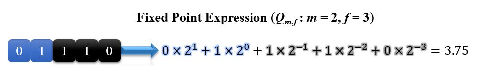
Figure 2. Fixed-Point Expression
C. HDMI Interface
We attempted to leverage an HDMI daughter board to output a higher resolution (1280x720 “720p”). The daughter board was designed by Terasic and contains an HDMI chip produced by ITE based on a CAT6613 Driver. The ITE chip requires very similar input signals as the VGA with slightly modified timings. The daughter board interfaces over the HSMC port available on the DE2-115. There are three interfaces carried by the HSMC connector, the digital video interface, I2S Audio Interface, and I2C Control Interface. Since audio wasn’t used in this demo, the I2S interface was ignored.

Figure 3. HDMI Block Diagram
Both the HDMI and VGA modules read the color / data from the color ROM and output to their respective displays. Even if both HDMI and VGA used the same timings (front porch, back porch, etc), their timing signals would have to be aligned so that they would read from the same XY location in memory. Due to this added difficulty in aligning the timings, it was chosen not to run the displays in parallel. Instead the system would either output to HDMI or VGA. Interfacing either the VGA or HDMI to the frame buffer would be the same.
Logical Structure
A. MandelBrot Calculation Core and Engine Design
The most difficult part of this project is to design an efficient calculation unit. Only if the calculation core is correctly designed, can the calculation speed be dramatically improved. There exists three main tasks to finish the fractal calculation:
1. Map the real display coordinates to complex plane;
2. Distribute the calculation task to calculation core;
3. Mediate the writing process of multiple data stream from calculation cores.
Based on this method,
the logical structure of our calculation engine is shown in Figure 4. The "Task Distributer" is responsible to calculate complex plane coordinates based on real display coordinates and send the calculated coordinates to calculation cores, as long as there exists one free core, it will always send the task to it, otherwise, it sends the task to the first core by default.
Generally, if there exists sufficient caculation cores, there should always exists a free core. However, due to the number of hardware multiplier limitation, we can only instantiate limited cores into the calculation engine. This means that the first core may be overloaded, to solve this issue, a FIFO is implemented as a bridge between the cores and the task distributer. In this scenario, all tasks are buffered, even though there's no free cores in current cycle, there may exists one free core in next cycle, then the task executer will re-arrange the task in the FIFO to that free core.
Even if we can guarantee that all cores are busy in each cycle, how to arrange the scattered data flow to write to SRAM would still be an issue. To solve this issue, every calculation core is equipped with private FIFO, and the "Results Mediator" is responsible to appropriately fetch the result from different calculation cores and write it to SRAM.
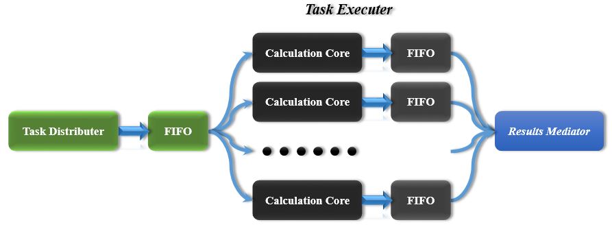
Figure 4. Calculation Engine Logical Structure
B. FFT Implementation
We successfully implemented two different FFT modules into our design, one module is "cFFT" from OpenCore, and the other is "MegaCore FFT" from Altera. Both of these two modules are able to calculate 1024-point FFT efficiently except for different hardware consumptions. The logical structure of FFT part is pretty simple. FFT module is connected to the audio streaming port, then a simple normalization unit is responsible to fetch the FFT analysis results and finally map the maginitude in different frequency points to color palette. The block diagram of FFT part is shown in Figure 5.

Figure 5. FFT Logical Structure
Relevant Standards
This project uses IEEE standards for Verilog which is ensured by the Quartus compiler.
Hardware Design top
The whole project is implemented in hardware, pipeline and parallelism strategy is widely used in design. In this section, we will talk about three core units of our design: Calculation Core Design, Calculation Engine Design, Mediator Design and FFT Analyzing Unit Design.
A. Calculation Core Design
As described in section "Logical Structure", calculation core needs to be appropriately designed to decrease the calculation time and finally improve the overall performance. Generally, we would like to apply clock with high frequency to the core to achieve this target. However, we must also pay attention to the critical path during the design process. If the negative slack of the critical path (critical path cannot accomodate high frequency) is too large, we won't be able to get high performance. The main calculation parts in the core would be adders, substractors and multipliers. We added different number of pipeline stages of these units to make sure that it can run in higher frequency. Notice that there always exists trade-offs between the number of pipeline stages and cycle time. In this project, we use Altera MegaWizard to specify the pipeline stages of multiplier as 5, for adder and substractor, the number of pipeline stages is specified as 2. The data path of the calculation core is shown in Figure 6.
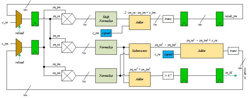
Figure 6. Data-Path of Calculation Core
Note that to guarantee the accuracy, we designed the truncate logic at the end of main calculation units. Meanwhile, considering that the embedded multiplier of EP4C115 is 9-bit, we use 36 bit (Q3.33) Fixed-Point math to achieve maximum performance and utilization. The multiplier performance of EP4CE115C7 is shown in Figure 7, generally, the cycle time becomes longer as the bit width of operands increases. Based on this figure, we can estimate that the maximum frequency using 36-bit multiplier would be less than or equal to 150MHz. In our project, we achieved 130MHz performance.

Figure 7. EP4C115C7 Multiplier Performance
The control logic of calculation core is pretty simple, most control signals are generated via combinational logic instead of FSM. The calculation core will pass the display coordinates through itself and output the number of iterations. The result is stored into its private FIFO.
B. Calculation Engine Design
The calculation engine instantiates multiple calculation cores to realize parallel calculation. As refered in section "Logical Structure", the caculation engine unit also instantiates a FIFO to receive complex plane coordinates, it also instantiates multiple private FIFOs (Back-End FIFOs) to buffer the results (number of iteration) generated from calculation cores. The datapath of calculation engine is pretty intuitive, please refer to Figure 3 for its simplified datapath.
Even though the calculation enginer is just a task dispatcher, it must dispatch tasks fast enough to make sure that all calculation cores are busy in every cycle. Based on this point of view, we used for loop to generated parallel busy detection and task dispath logic. By doing this, we can guarantee that as long as there exists unfinished tasks in the Task FIFO (Front-End FIFO), all the calculation cores would be busy in every single cycle.
C. Mediator Design
The mediator aims to execute three main tasks:
1. Calculate the complex plane coordinates based on actual display coordinates;
2. Fetch result from Calculation Cores' private FIFOs and store it to SRAM;
3. Modify complex plane coordinates based on user's PAN / ZOOM command.
Note that in Figure 1. System Block Diagram, the mediator is splitted into two parts: "Fractal Display Control Core" and "Data Flow Bridge (Mediator)" for clarity.
There's no data path of Mediator, but it includes two simple FSMs for SRAM Write Control and FIFO Update Control. Figure 8 shows the Front-End FIFO Update Control FSM while Figure 9 shows SRAM Write Control FSM.
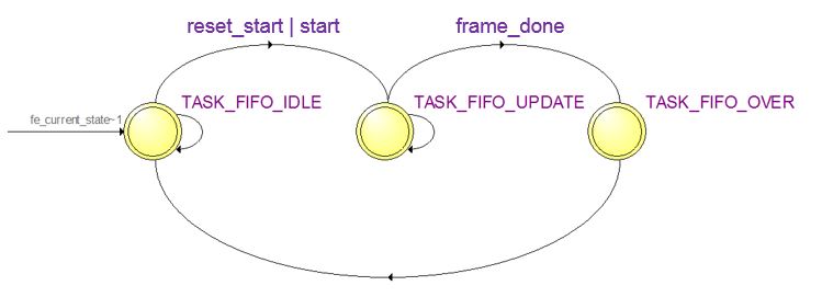
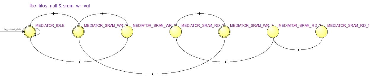
Figure 9. SRAM Write Control FSM
Please note we implemented two SRAM control strategy for High-Resolution Display. With 1024x768 resolution and 16-bit iteration, the video buffer size would be 1024x768x2 = 1.5MB. However, if the resolution is higher, we would have no choice but to use RMW (Read-Modify-Write Method) to indirectly update the SRAM. Since the RMW would hurt the performance dramatically, we used Write-Only method to guarantee the update speed.
D. Control Interface Design
The PAN / ZOOM operation can be either realized by using UART / IrDa Remote Controller. Considering that IrDa Receiver may be interfered by fluorescent lamp. If we simply combine these two signals together using OR gate, then if IrDa is interfered, the control signal would be unstable. To avoid this problem, several 2-input multiplexers are implemented to select control signal source.
I. Auto-Baud UART
This UART module scans the data stream from serial port. Since a new character always starts with a "START" bit (Logic "0"). When the "START" bit is captured, an internal measurement process starts, trying to determine the BAUD of incoming character. Different characters have different bit transitions, thus, to make sure the measurement circuit can correctly recognize the BAUD, user must input several identical chacters. As soon as the measurement circuit get the same character more than 5 times, it will use the last BAUD configuration to start the BAUD generator. After that, the module will decode the character from serial interface and echo the character it receives to user. A UART decoder module is implemented to map user's command to PAN / ZOOM signals.
II. IrDA Remote Control
Similar to UART module, the IrDA control module is composed of IrDA controller and corresponding decoder. The controller is designed based on IrDA specification. It will output a ready signal when it successfully decodes a valid key value. The IrDecoder will then take this key value and map it to either PAN or ZOOM command.
E. HDMI Control
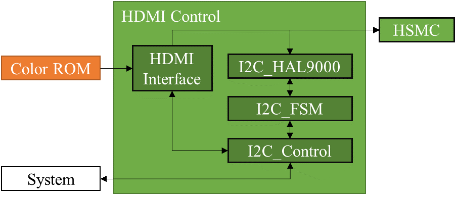
Figure 10. HDMI Implementation
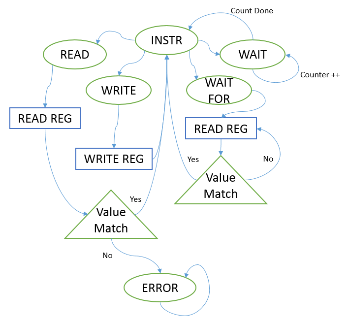
As shown in Figure 10, the HDMI chip is controlled over an I2C bus and uses an interrupt pin to indicate when an event has occurred. As illustrated by the HDMI Control block, the I2C interface was built out of three compounded state machines. Each state machine represents a higher level of abstraction. The Hardware Abstraction Layer (HAL) handles the I/O timings and toggles the lines according to its instructions (read, write). The finite state machine (FSM) handles the repetitive tasks of sending an address, writing the register value to either be modified or read from, and then repeating this to read or modify said register. The Control state machine operates similar to a CPU with limited instructions as illustrated below (Figure 11).
 |
 |
 |
| High Level Control | FSM | HAL |
Figure 11. HDMI Control FSM
As shown above, the high level control state machine is able to read an array of commands and perform operations. This enabled fast debugging and easily modify the behavior of the state machine to interface to the ITE chip.The ITE chip has over 256 registers used to configure the chip. Since the number of registers exceed the maximum number addressable by an 8 bit value, a bank register is used. This enables two banks of registers.
F. FFT Analyzing Unit Design
Sound waveforms can be modeled as the sum of harmonically-related sine waves. The Fast Fourier Transform aims to decompose those since waves into their sine components. Instead of using time as x axis unit, Fast Fourier Transform use frequency as x axis unit. Since our project aims to use audio sound to adjust the Mandelbrot set, we have to use fft to get the amplitude at each frequency and then use those values to map to different color.
I. OpenCore cFFT
cFFT is a radix-4 Fast Fourier Transform core with configurable data width and a configurable number of sample points in the FFT. The block diagram of cFFT is shown in Figure 12.

Figure 12. cFFT Block Diagram
To use cFFT, we just need to know the input and output timing. Compared to Altera MegaCore, cFFT simplify the interface and make it more easy to use. Figure 13 and Figure 14 shows the input and output diagram of cFFT.
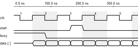
Figure 13. cFFT Input Timing
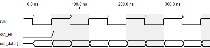
Figure 14. cFFT Output Timing
Note that, the output sequence of cFFT is 2-bit reverse ordered. For instance, the 789th (1100010101) output in an 1024-point FFT is actually at 339 (0101010011).
II. Altera MegaCore FFT
Altera already build a multifunctional FFT IP core, and we choose a Fixed-Point Variable Streaming FFTs as our fft module. Our fft module take 18 bits from audio (16 bits with sign extension) as real part input and zero as imaginary part of input, fft module output a 29 bits output for both real and imaginary part. The detailed input/output information of our fft module is shown in below (Figure 15).
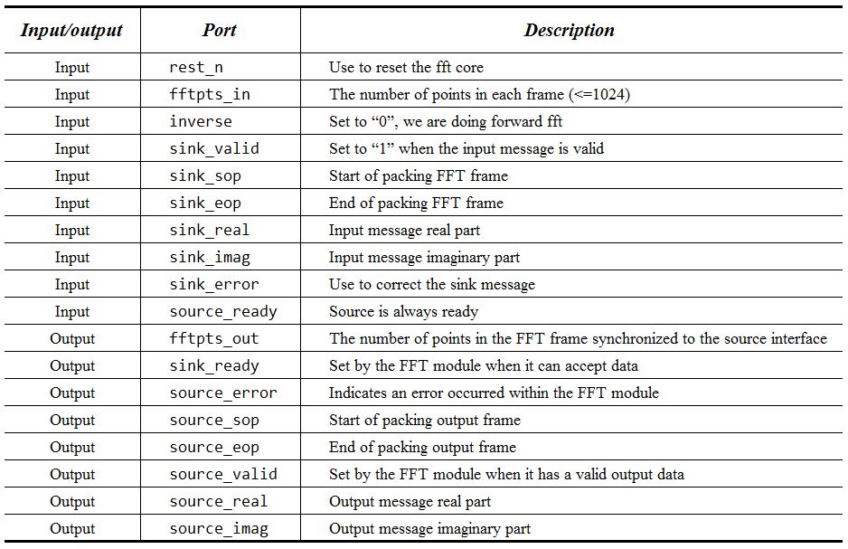
Figure 15. Altera MegaCore FFT Interface
Since the input message sent into the fft module is as frame, and the fft module can be run way more faster than the normal audio module. We add an additional 18 bits rom with 256 entries to store the audio input data and then use another 8 bits 256 entries rom to store the output data. A brief block diagram is shown in Figure 16.
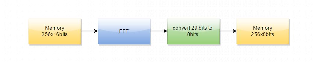
Figure 16. FFT Analyzing Unit Block Diagram
However, we encountering a problem of convert 29 bits output data to 8 bits data and we lost the accuracy of the output data. The data stored in output rom make the color for each iteration very similar.
Software top
Before we start implementing the real fft core, we use java and matlab to simulate the animation of Julia set (Julia set and Mandelbrot set are both using the iteration of polynomials and rotational functions to display the image). The simulation process is briefly shown in Figure 17.

Figure 17. Software Simulation Process
Java Simulation
The animation of Java simulation was shown in below, the left animation is using random data to set the array and then use the number of iteration as index to read the number and set it as the red color (R:0~256). In order to reflect the color change at different iteration, we only use red color and set green and blue as zero.
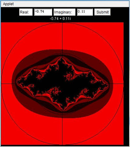
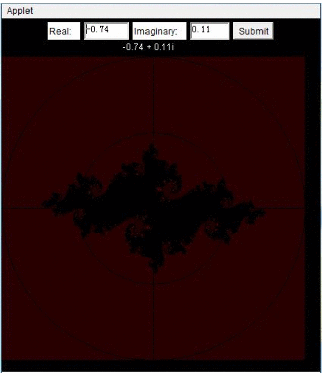
Figure 18. Java Simulation Animation
The left animation use the real output data to map the red color, as you can see in the animation, the pattern is really dim, because the converted output data is relatively small. In order to make the animation more contrasted, we have to update the look up table for converting a 29 bits number to an 8 bits number.
FFT Spectrum Color Mapping
As mentioned above, how to better map the FFT results to color space is very important in our design. To guarantee that we can see the color can dynamically follow the FFT audio spectrum, we implemented several color schemes and store them into a color RAM so that it can be modified in RealTime. Since the cFFT output the magnitude sequentially, the output data's index is mapped directly to the number of iterations output from calculation engine. In this way, cFFT is able to change specific color inside different color schemes. In other words, cFFT will change the RGB color based on the magnitude in different frequency points (magnitude => RGB value, Frequency point => Color Index). This idea is shown in Figure 19.
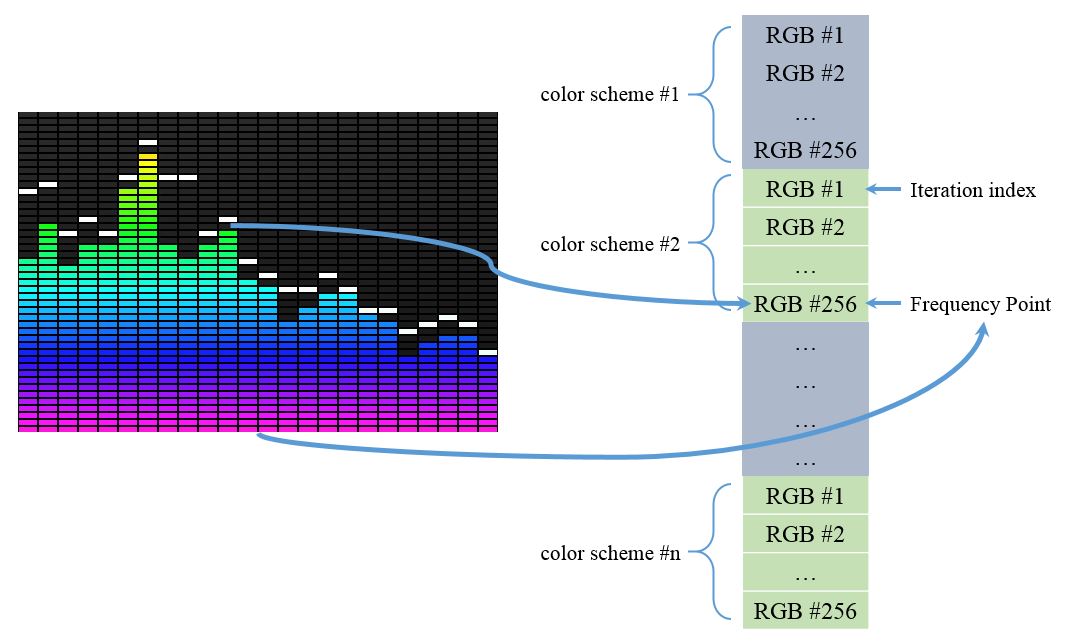
Figure 19. Map FFT analysis results to color space
Results top
MandelBrot Calculation Parallelism
To verify the original parallel design purpose, we use SignalTap to explicitly monitor calculation cores' status to validate whether the parallel strategy. Figure 20 shows the output from calculation task dispatcher (calculation engine fetch the task and dispatch it to available calculation cores).
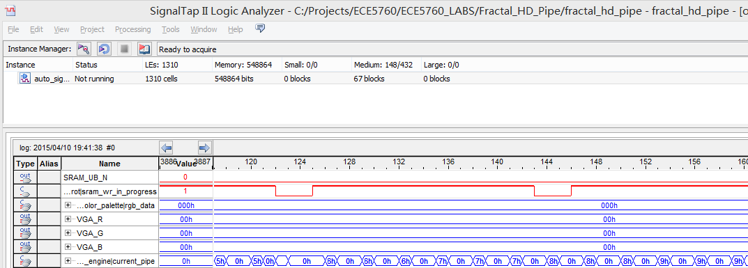
Figure 20. Calculation Task Dispatch
From the SignalTap results we can see that the dispatcher can successfully assign tasks to different cores based on their status (busy or free). However, calculation core 0 is selected more often than other cores, this is because when all cores are busy, we select core 0 by default. Based on this result, we can also observe the hardware limitation: If we have sufficient hardware multipliers, then all cores should be selected with same probability.
Altera MegaCore FFT Accuracy
In order to verify the accuracy the fft module, we first use modlesim to simulate 15 packets and each packet contains 256 elements. As the red and yellow box shown in the figure, the sink sop/eop and source sop/eop correctly assert 15 times. After the modlesim generate all ouput data, we use the provide matlab testbech with same input data set to verify the correctness of the fft core. After we verify the functionality of the fft module, we start putting the fft module with the audio interface together and use 18 LEDs on FPGA to reflect the fluctuation of the music, those 18 LEDs are act as a music spectrum. Those LED are select at index 14, 28, 42, 56, 70..........225, 239, 253 and if the number stored in that specific index larger than 100, we turn on the corresponding LED, otherwise, we turn off the LED.
When we saw the “LED music spectrum” varied with music, we are ready to connect the fft module with the VGA controller to select the corresponding color. The video is shown below (LINK will be added later).
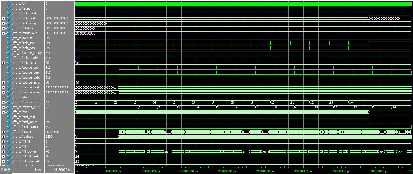
Figure 21. ModelSim FFT Simulation
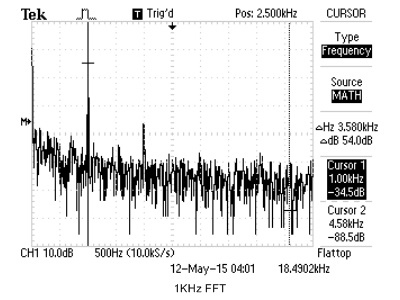
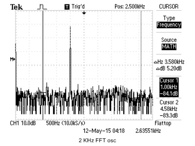
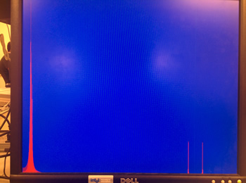
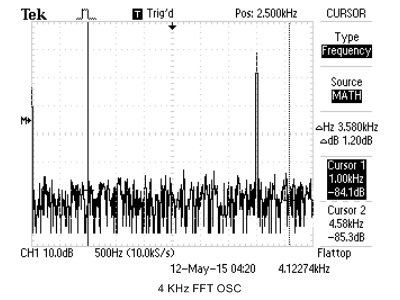
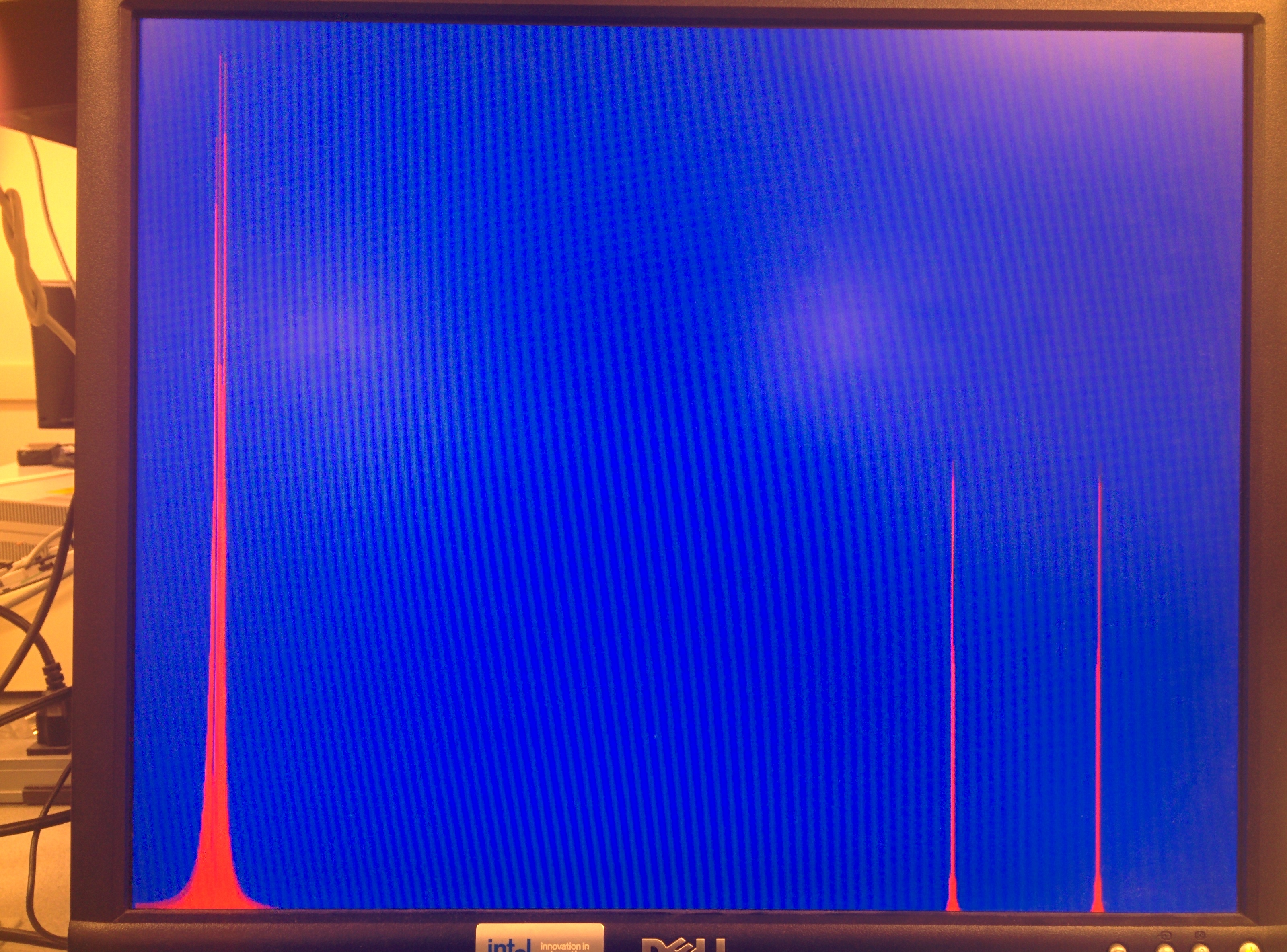
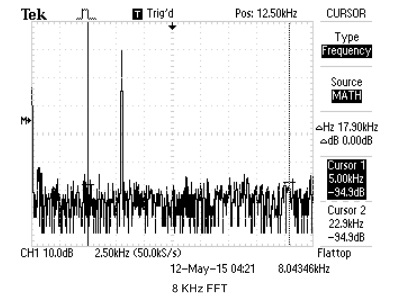
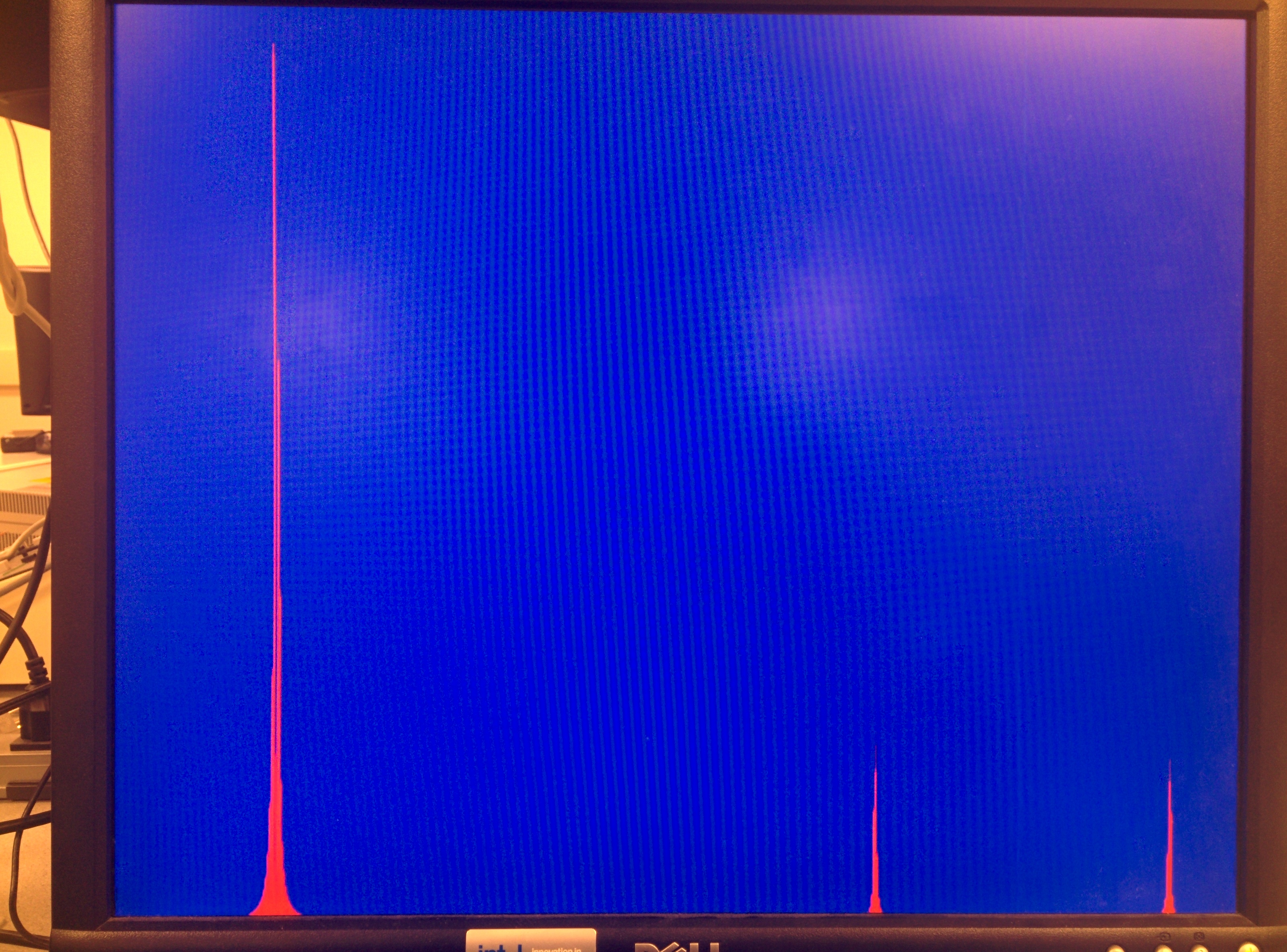
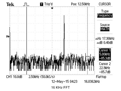
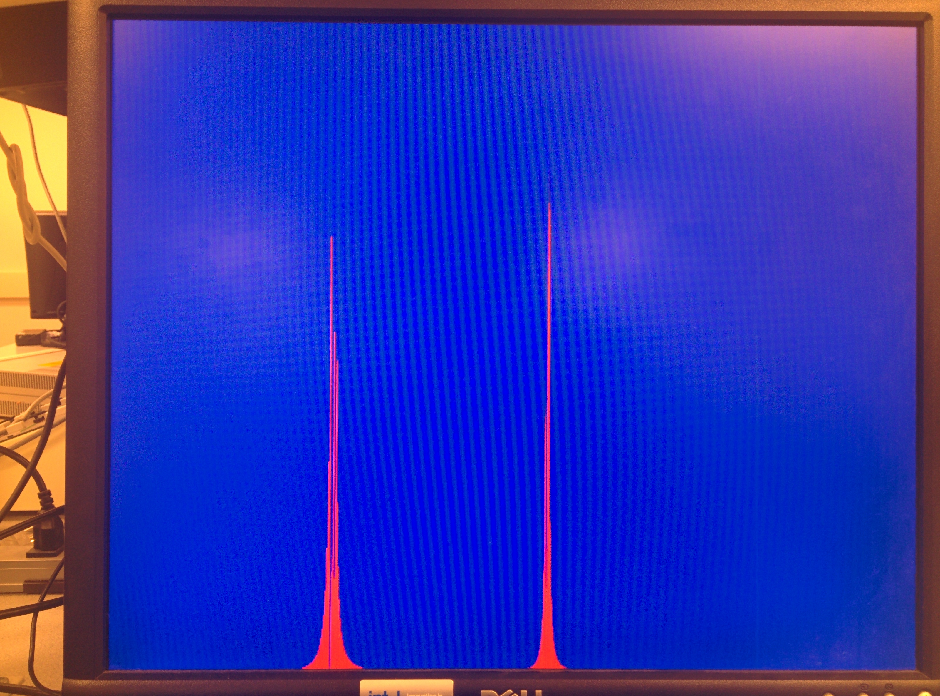
cFFT Accuracy
We use cFFT to build a spectrum analyzer, with a standard online tone generator, we are able to compare the cFFT results to real oscilloscope's FFT output. For simplicity, we just use sine wave to verify cFFT's functionality. The results are shown below.
 |
 |
| 1KHz OSC | 1KHz cFFT |
 |
 |
| 2KHz OSC | 2KHz cFFT |
 |
 |
| 4KHz OSC | 4KHz cFFT |
 |
 |
| 8KHz OSC | 8KHz cFFT |
 |
 |
| 16KHz OSC | 16KHz cFFT |
Figure 21. cFFT Verification
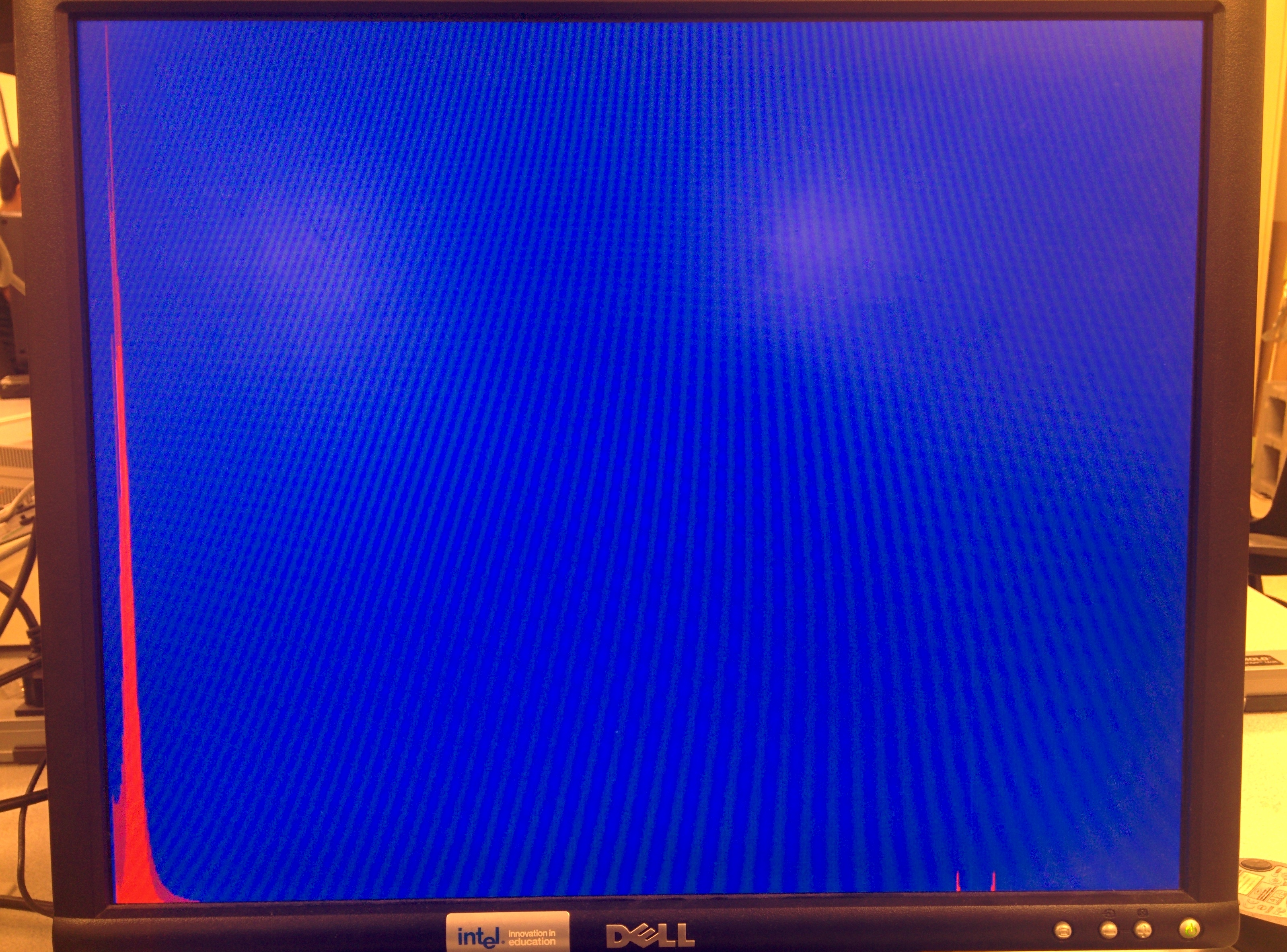
HDMI Validation
Terasic provided a very elaborate HDMI demo that detects the different modes of the HDMI display and cycles through different resolutions using a test pattern. Unfortunately, their implementation of the i2C interface uses the NIOS II soft-core processor and has over 5,000 lines of C code to configure the chip.
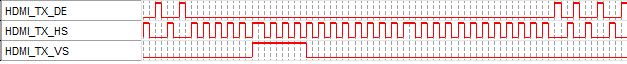
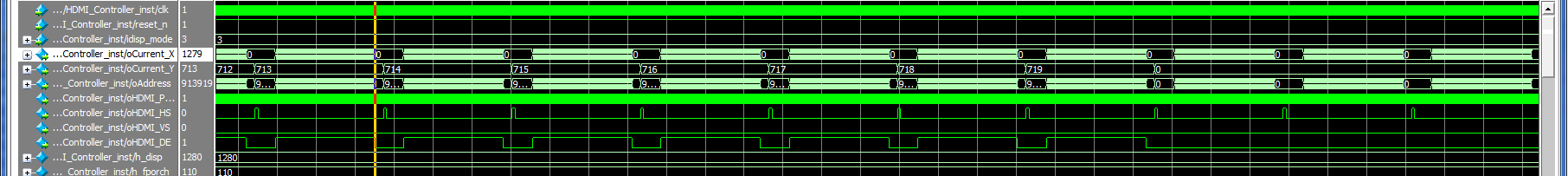
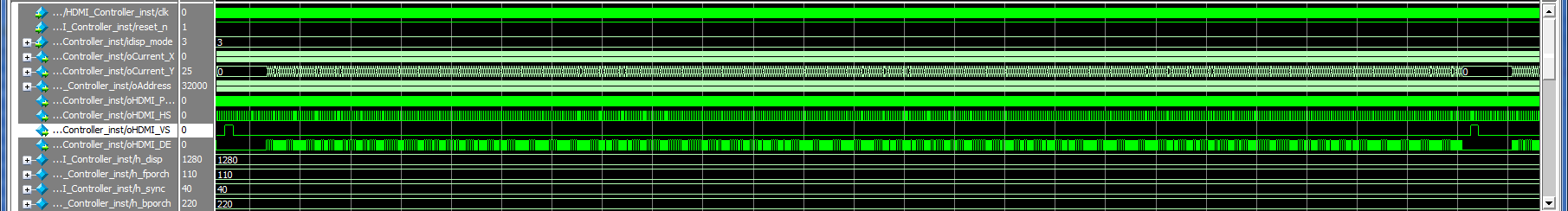
Figure 22. HDMI Verification
Terasic used Verilog to control the digital video interface between the FPGA and ITE chip. This Verilog, also overly complicated, was extracted from their demo and used. However, even though timings matched up, the ITE chip reported that the video signal was unstable. This prevented the HDMI control from being able to “Fire” or start the analog front end (AFE).
The ITE programming guide states that if V-sync, H-sync, and Data Enable (DE) aren’t used, registers can be programmed with the front and back porch values to generate the signals internally. Even with all sync signals enabled and internal registers programmed, the ITE failed to identify a stable video stream.
Both ITE and Terasic were very reluctant to help and instead defaulted to the “read the programming guide” or “use our demo”.
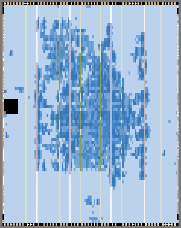
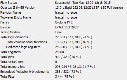
Quartus Synthesis Result
As shown in Figure 23, we consumed a lot of hardware multipliers since there exists 16 parallel calculation cores. We didn't use much LEs since there's no complicate control logic of our project. Based on this result, we can still see some future improvements.
 |
 |
| Overall Chip Planner | Synthesis Report |
Figure 23. Synthesis Report and Chip Planner
Conclusions top
In this project, we implemented an efficient HD Mandelbrot set display. Our original idea of this project is to dynamically zoom in / out the Mandelbrot set based on FFT analysis results. However, it would be very difficult to achieve this due to the time consumed on massive calculation with HD resolution due to hardware limitations (hardware multiplier quantity, on-board SRAM / LE / M9K). With current implementation, the screen refresh speed is limited by two main factors: Single-Port SRAM and the number of hardware multipliers. With more hardware multipliers we can implement more calculation cores to achieve higher calculation parallelism. If we have sufficient on-board M9K blocks, we can directly use dual-port RAM (M9K/LEs) instead of using single-port SRAM. The trade-off between hardware limitation and the degree of parallelism always exist in hardware design.
Meanwhile, we also successfully map the FFT results to color space. As shown in the video, partial color is changed while other color stays still. In this scenario, we can clearly see that both the color density (magnitude) and color area (frequency point value) is changing with the music.
Future Works
- Fix HDMI current configuration bugs and try to display mandelbrot set with 720p or higher resolution;
- Display MandelbrotSet parameters on screen;
- Display MandelbrotSet calculation speed on screen;
Intellectual Property Considerations
Altera MegaCore FFT.
Appendices top
A. References
-
OpenCore cFFT
- Altera FFT IP Core
- Real time speech recognition engine project from ECE5760 fall 2010
- OpenCore AutoBaud Rate
- IRDa Specifications
- Implementing Filters on FPGAs
- Altera Cyclone IV Handbook
B. Source Code
Please contact Wancheng Zhou (wz233@cornell.edu) for source code request.
C. Tasks
| HDMI Transmit Part | Joseph |
| Mandelbrot Set Calculation Architecture Design | Wancheng |
| cFFT Core Implementation | Wancheng |
| Altera FFT Core Implementation | Lu / Wancheng |
| Software Simulation | Lu |
| System Testing & Verification | Joseph |
| Website Report | Wancheng |
Acknowledgements top
We would like to thank our mentor Bruce Land for his guidance, trust and encouragement. Thanks our TA Deepak Awari for his guidance and suggestions during our labs.