High-Level Hardware/RTL Design
Note that modules discussed may not be exact representations of our RTL, but are high-level overviews of how our RTL is structured and interactsNode
The most basic module in our structure is a node. This module implements the automata logic; it takes in the current state of a cell, as well as the current state of the cell's neighbors, and computes what the next state of the cell should be:
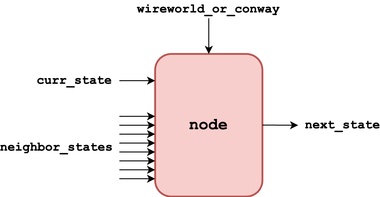
We initially implemented this to solely operate on states; however, with the late addition of Game Of Life functionality, we included another input, wireworld_or_conway, to determine which automata our update logic should follow. This was connected to a switch on the FPGA, allowing the user to switch between automata with ease.
Iterator
Once we have our node, we can instantiate inside of an iterator. An iterator is responsible for iterating across an entire row of state, providing the new states for cells as it iterates along:
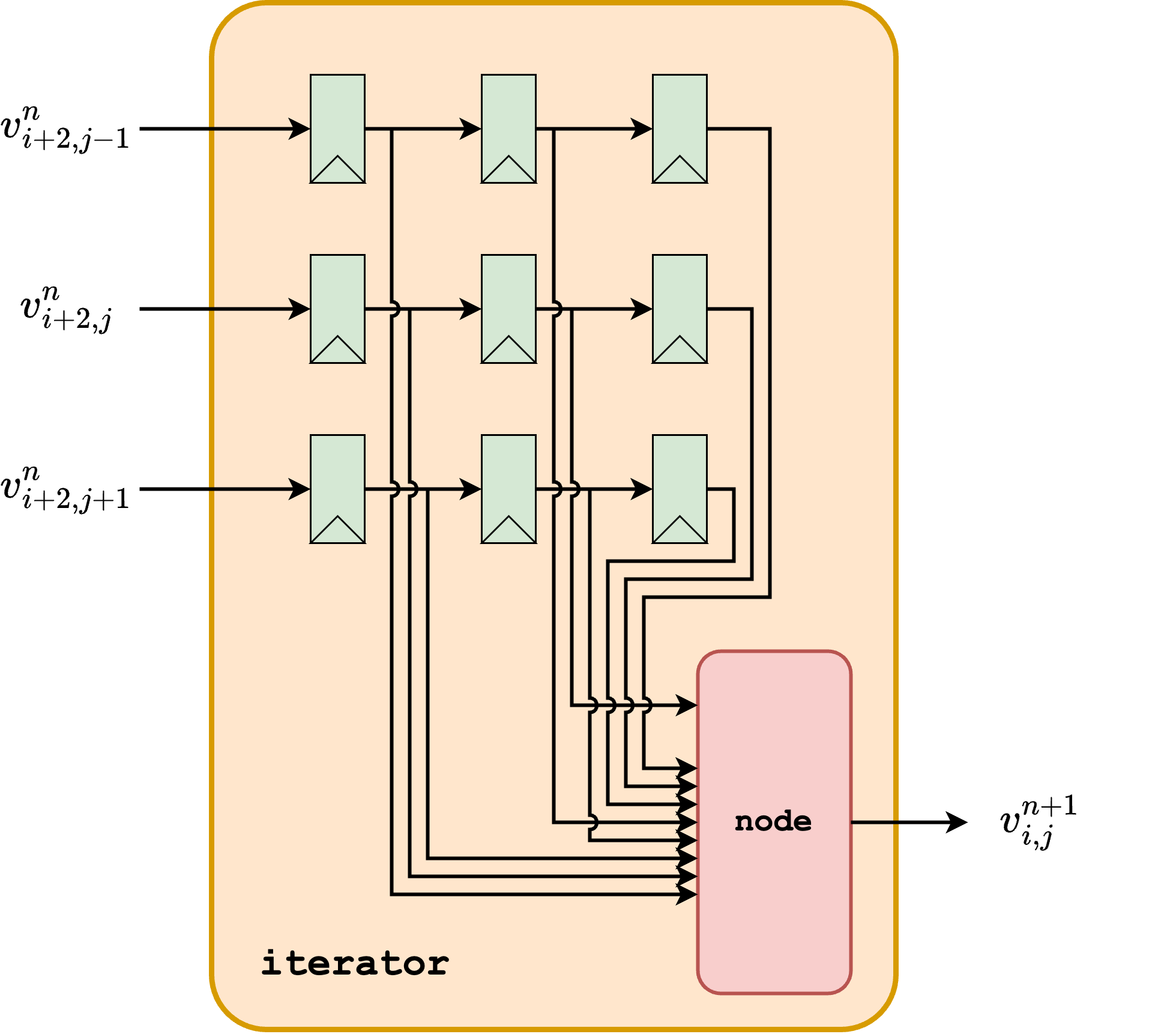
Here, we can see that the iterator pipelines the state it reads in order to feed the current state of a cell and its neighbors to the node; the iterator will always be reading two steps ahead of the cell that it's computing the next state for. This has the side benefit that by the time we write new state back to memory, we have already read it into the iterator, guaranteeing that we won't be reading back the new state we just calculated.
Column
Each iterator is intended to iterate across a single row of state. To update the entire state, we need a column of these iterators, each responsible for a designated row. This diagram is shown below; the columns are fed in the data (rvals) from the same address (raddr), ensuring that they update state in lockstep and allowing the new state (wvals) to be written to the same address (waddr) using a write-enable signal (we). Here, addresses correspond to a particular column, with the value for each row in the column being read in parallel.
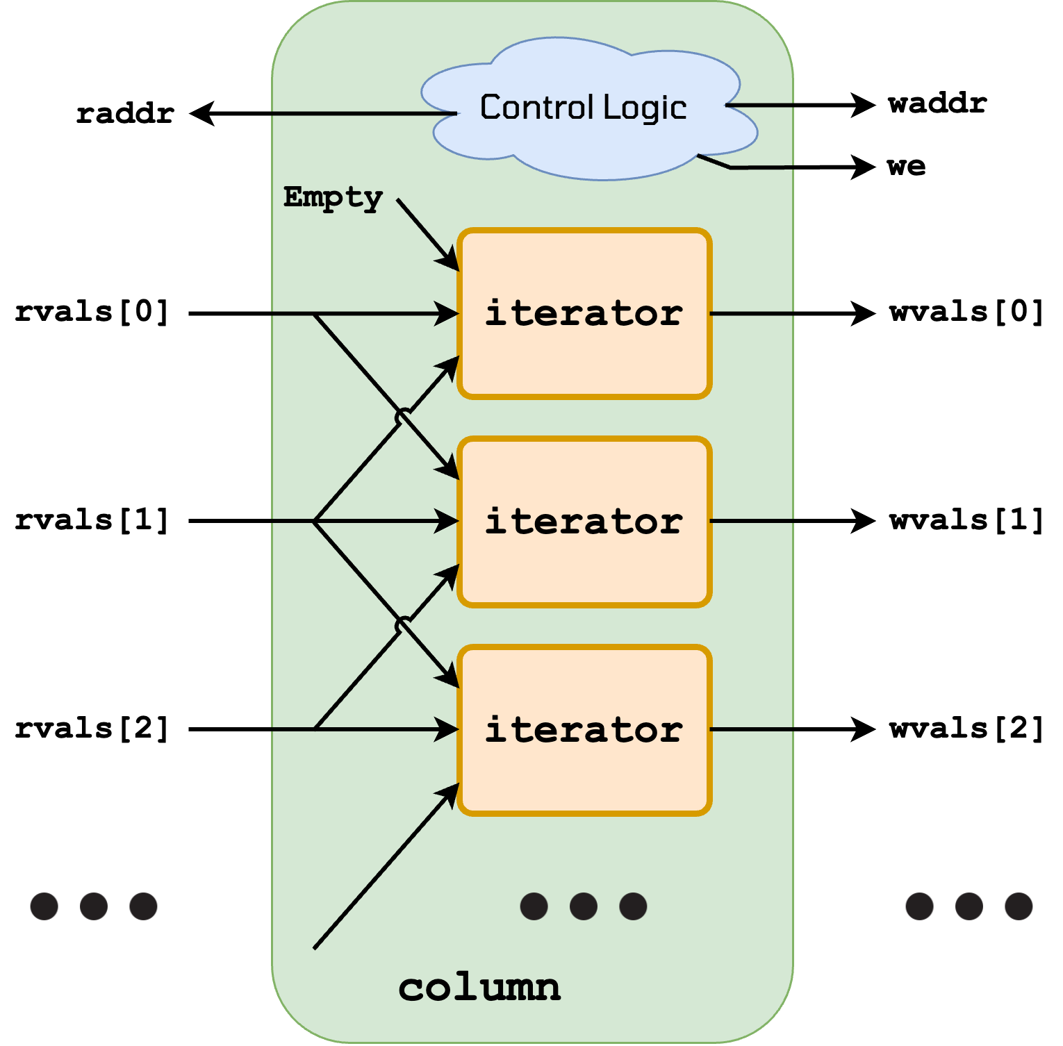
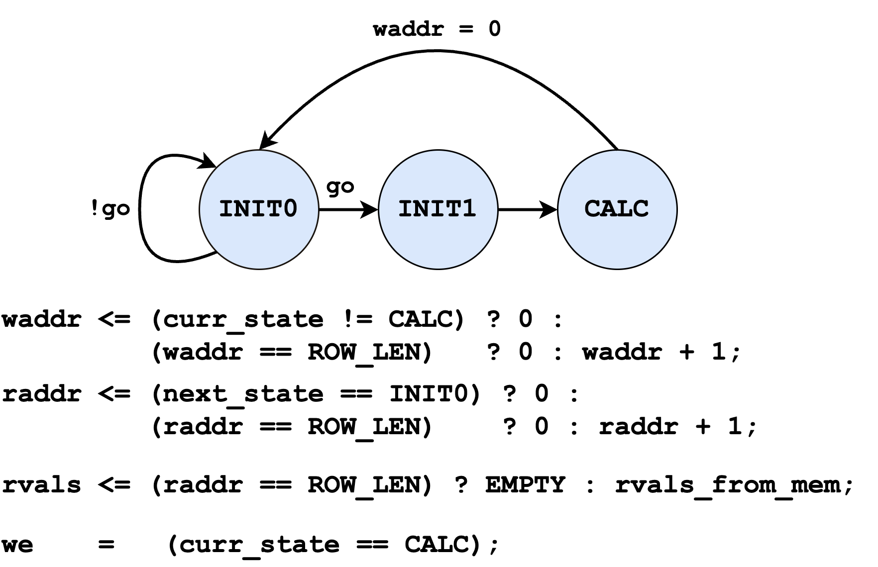
Here, control logic is necessary to determiine the correct addresses to read from and write to, especially noting that we need to feed in extra Empty values whenever we are at the beginning or the end of the grid to avoid wrapping around. We implement this control logic using an FSM, which has INIT states to feed in these extra empty values, and which updates a counter to keep track of where we should be reading from and writing to.
Notably, we allocate one bit more than is necessary to address the entire row, to allow for iterators to take in Empty when we go beyond the row length. Whenever raddr = ROW_LEN, we inject an Empty value into our iterator pipeline, to make sure that the end of a row (and the beginning of the next row) is interpreted as Empty for the automata.
Not shown: The go signal comes from the HPS. When the HPS wants to have the solvers update, it will set this register to the number of updates to perform. The solvers check this register in INIT0, only progressing when it's high (and decrementing by 1 when it progresses to INIT1). Lastly, the go signal sent from the register to the solvers is only high at the beginning of the horizontal blanking state, discussed below. This ensures that we only start an update at the beginning of horizontal blanking; since this state takes 45 rows * 800 pixels/row = 36000 cycles, this ensures that the entire state can update before horizontal blanking is over (and we lose the ability to write).
Mouse Interface
To interact with our design, we use a PS2 Mouse, allowing us to control it directly through the FPGA. To do this, we use an external piece of IP to interface with the PS2 protocol, giving us the current location of the mouse, as well as when the mouse is clicked:
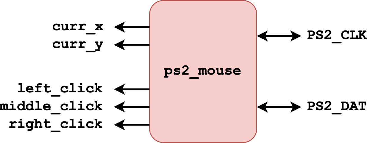
The main interaction that we perform with the mouse if using it to update memory. For this, we use a write buffer, which translates the current location into a memory write when the mouse is clicked (complete with an address, a value, and a write-enable based on which row we're writing in the addressed column). In this way, the buffer is responsible for translating a given coordinate into the cell that we want to write to.
The reason we call it a "buffer" is because there are some other underlying signals that cause mouse writes to buffer; specifically, when we receive a click, we wait until the corresponding location is read, so that we know what the next state should be (with mouse clicks cycling through all possible cell states). However, the mouse doesn't necessarily control these signals, but rather sniffs what is already being read, so they are omitted for brevity.
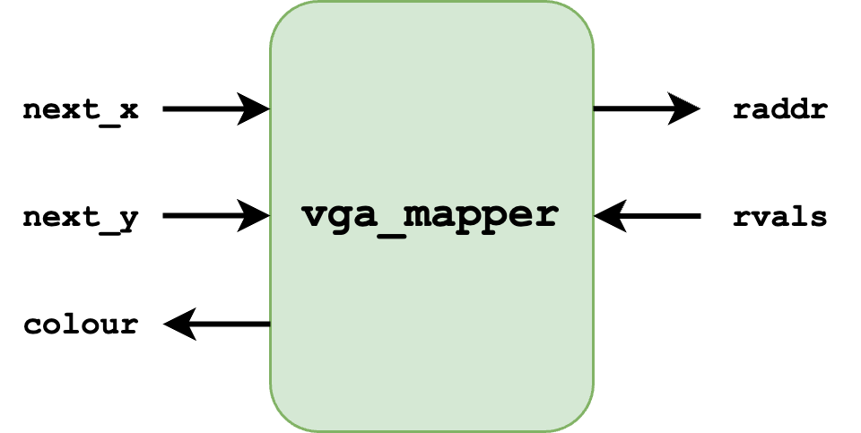
VGA Interface
In addition to the PS2 Mouse, the other external hardware that our design interacts with is the VGA screen. To perform this interaction, we were able to re-use Professor Adams' VGA Driver that was used in Lab 2; since we already understood how this piece of IP worked, we were able to integrate it into our project smoothly (albeit modified for full 24-bit color)
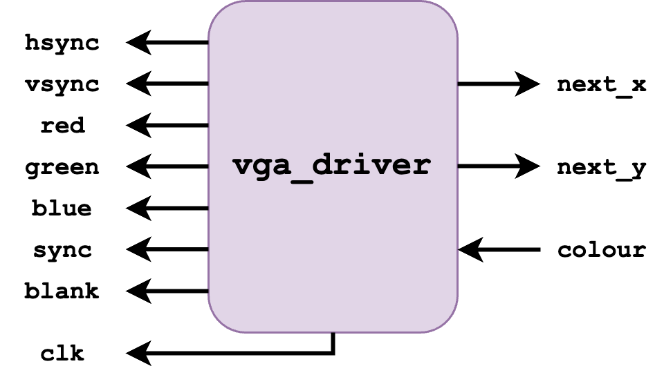
To fully integrate this driver into our design, we needed to have a VGA Mapper. This module was responsible for mapping the coordinates that the VGA requested to cells in our memory, similar to the mouse write buffer. In addition, it also detected whether we were near the "edge" of a cell, and always gave the colour grey if so (similarly, always giving the colour purple if the requested cell wasn't valid, given by the parametrized size of our cell grid).
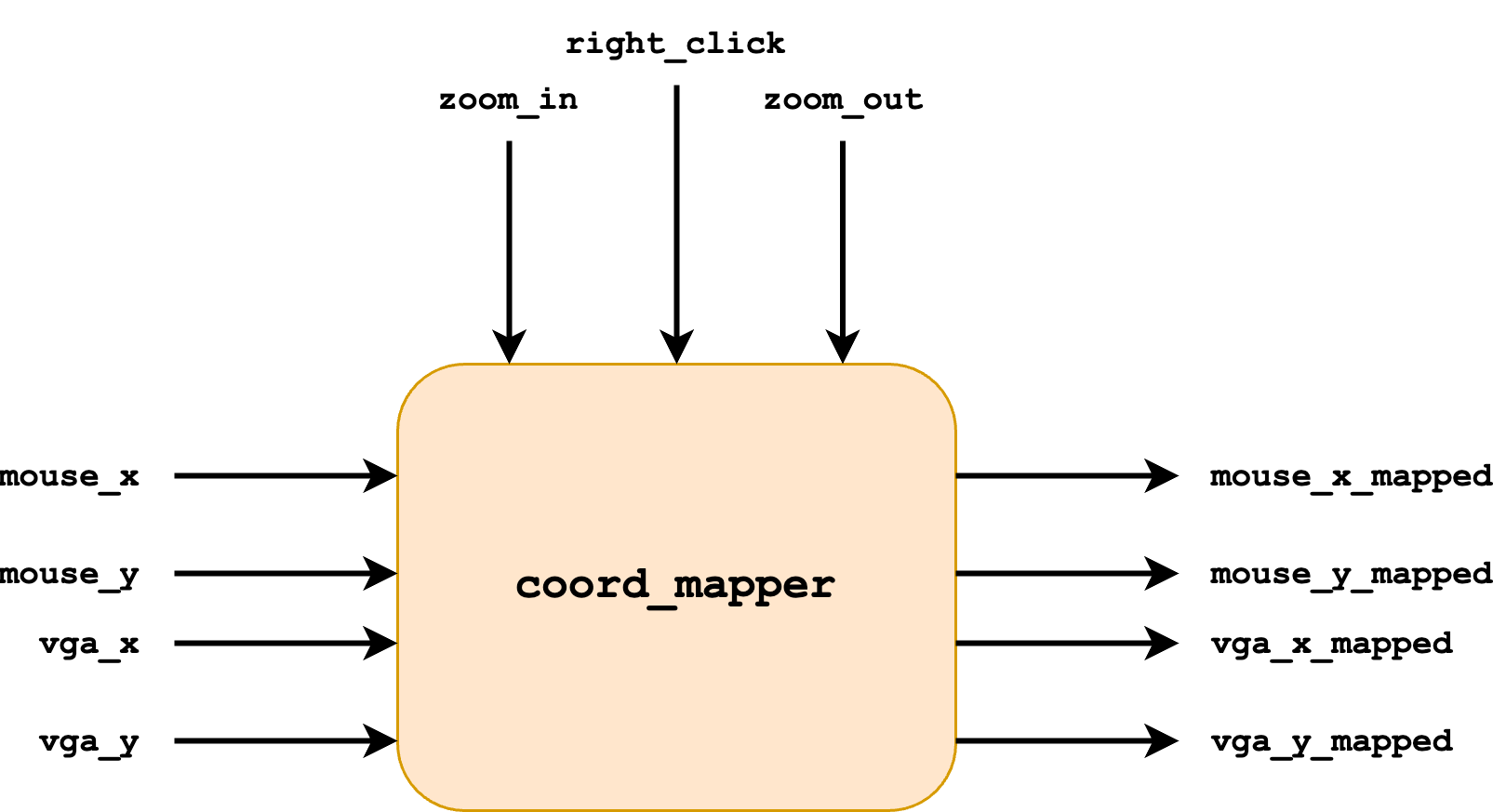
Coordinate Mapping
Normally, one could hook up the mouse interface directly to the write buffer; similarly, one could connect the VGA driver to the mapper. However, in our design, we wanted to implement zooming and panning. This requires an in-between module to translate the initial input coordinates into "mapped" coordinates that reflect any zooming or panning that has occurred.
For our design, zooming is done through the use of two FPGA buttons. Panning is done by holding the right mouse button while moving the mouse, so that users can drag to move across the grid of cells. Our coordinate mapper module takes these as inputs to keep track of the current zoom and pan amounts. From here, it can translate the input VGA and Mouse coordinates into their mapped versions to reflect the zooming and panning that the user has done. These will be fed into the mouse write buffer and VGA mapper instead, so that they operate on the desired, mapped coordinates.
HPS Interface
The last interface that our automata state has is to the Hard Processor System (HPS). Here, we want to allow user code to also be able to read and write state. This is done using PIOs (the protocol for which is described with the user program). The HPS Interface is responsible for turning the signals from these PIOs into read and writes to memory, using a similar address-value combination that is used with other modules. Notably, the HPS operates on absolute cell values, not screen coordinates, so no translation is necessary.
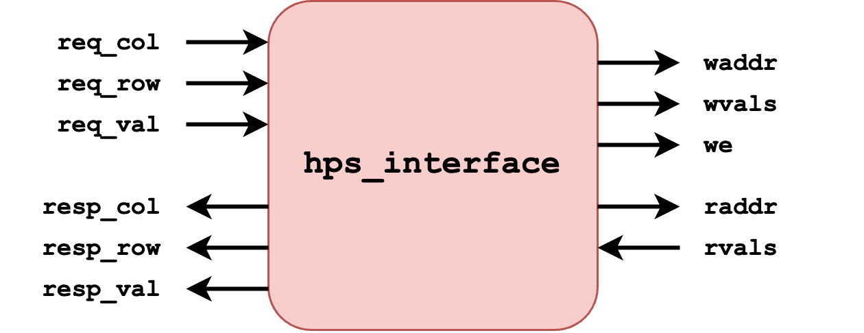
At a high-level, when the HPS interface receives a request on the request PIOs, it performs the action, and updates resp_row and resp_col to match req_row and req_col when the action is done, indicating that the HPS can move on. More detail is given on the Program page.
Memory Organization
A large component of our design is how we're storing the automata's state; we do this with M10K blocks. Each cell needs 2 bits to represent 1 of 4 states, meaning that with the M10K capacity, we can store the state of up to 390 * 4K = ~1.5M cells (although we limited ourselves to 1 million cells for our final implementation, on a 1000x1000 grid).
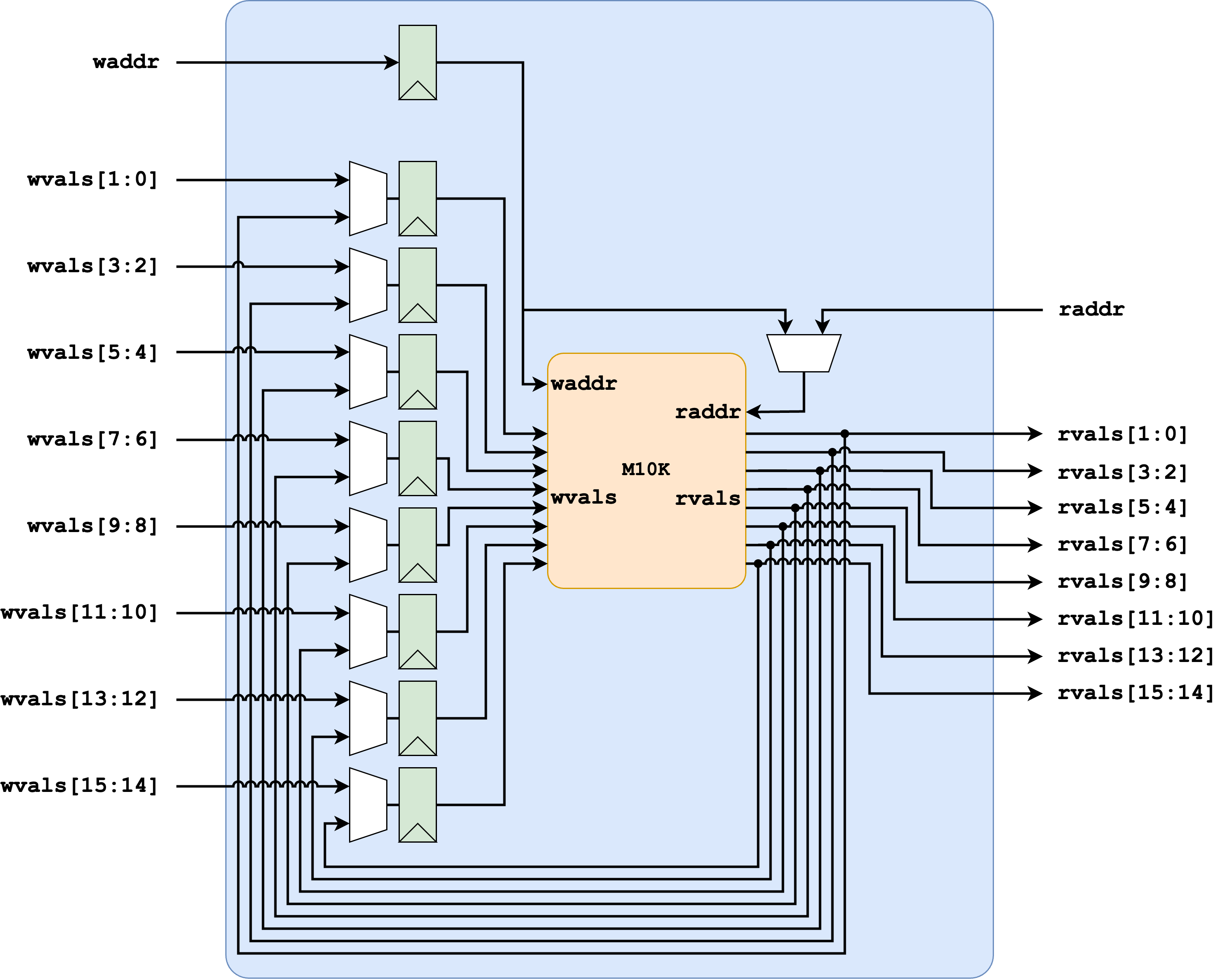
Initially, we assigned each iterator to an individual M10K block; however, this limited our aspect ratio, as we could only have 390 iterators, and therefore 390 rows in our grid. To achieve our desired 1000x1000 grid, we mapped 8 iterators to 1 M10K block. To do this, we had a write buffer before the M10K block:
- If all 8 entries for a given column were being written (such as when the iterators are running), then the write would be registered, and then immediately written back the next cycle, putting in a pipeline stage before the write. Since we never immediately read after writing a location, this still allowed for full throughput.
- If only 1 entry in a given column was being written (such as on a mouse click or HPS write), the value would be registered. At some later point, the corresponding entry would be read our, updated with our new value, and written back. This is necessary to avoid losing data; if we write only 1 entry, we don't know what the other 7 should be, and must therefore read their current value to know what data we need to write back.
This is implemented as a memory wrapper, surrounding each M10K block. Note how the values being read have the option to be registered as the next values to be written. Additionally, we keep track of the write address, and have the option to use it as the read address, in the case where we need the remaining data.
System Composition
The primary difficulty in composing the system is organizing our memory access pattern. We have many elements that want to be able to read and write state:
- Read: Solvers, VGA, HPS, Memory Wrapper
- Write: Solvers, HPS, Mouse, Memory Wrapper
To achieve this, we utilize the different VGA states. As the VGA iterates across the screen, the protocol requires a "blanking" region at the end of every row (vertical blanking), as well as for a few rows after the end of the screen (horizontal blanking), during which no data is sent to the VGA:
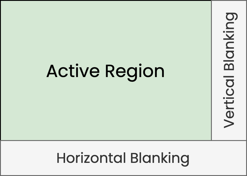
During these states, we define which modules are able to read and write (with the primary constraint being to have the VGA able to read data during the active regime). Modules must be aware of which state the VGA Driver is in, and not assume that their reads/writes will be correct if they're not in a state when they can read/write.
- Active Region
- Read: VGA Driver
- Write: HPS Interface (when active), otherwise the mouse interface
- This has the consequence that users can't use the mouse when the HPS is writing; since HPS writes are meant to be infrequent, we felt this was ok
- Vertical Blanking
- Read: Memory Wrapper (using stored write address)
- Write: Memory Wrapper (using stored write address)
- This is where we flush any partial writes by reading the current state, augmenting it with any values to write, and writing the entire value for 8 rows back.
- Horizontal Blanking
- Read: HPS Interface (when active), otherwise the (automata) solvers
- Write: The (automata) solvers
- This has the consequence that the automata won't update while the HPS is updating. This is preferable; otherwise, the solvers could update only the portion of currently-written state in the middle of a state write from HPS, meaning only part of our design will be updated
With this in mind, we can compose the entire system, with the VGA, Solvers, Mouse, and HPS all able to access state in memory:
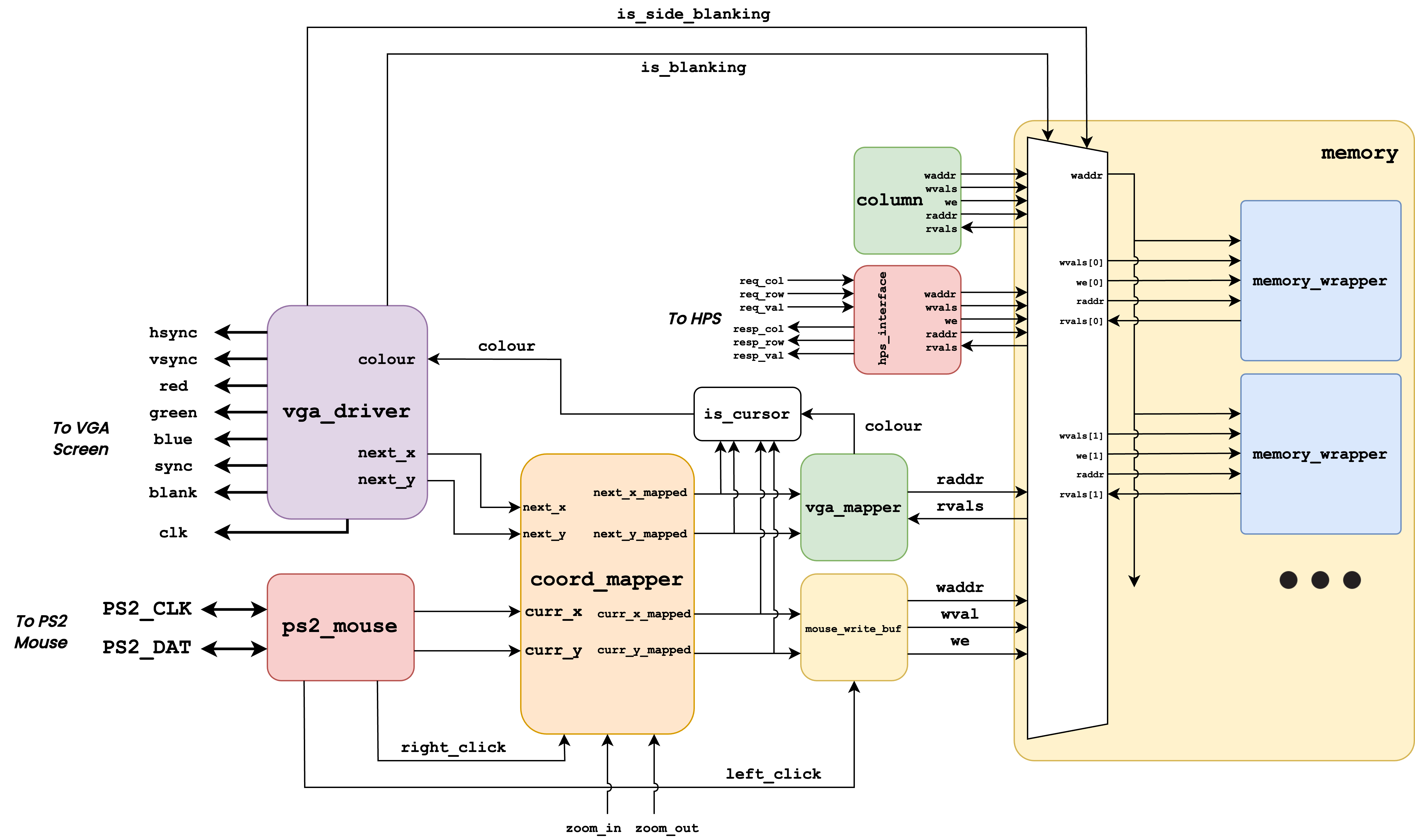
This includes some top-level logic that hasn't been previously discussed:
- The multiplexer in the memory block controls which modules get to read and write, according to the VGA state indicated by is_blanking and is_side_blanking, following our rules above. The control logic for each connected module also had these signals as inputs (not shown), to determine when it can make a valid read/write.
- The is_cursor block is to-level logic that checks whether the current coordinates we're looking at correspond to our cursor coordinates or near them; if so, we display different colors to indicate the cursor (and otherwise pass through the read color from memory). This allows us to display the cursor on top of our state, to indicate to the user where the mouse is.
- zoom_in and zoom_out are connected to buttons 2 and 3 on the FPGA, respectively.
- A "zoom" module isn't shown; this tracks the amount of zoom we currently have (incrementing and decrementing with button presses), and can be considered part of the coordinate mapper in the diagram.
- Some other control signals aren't shown that correspond to ease of use for the user:
- The wireworld_or_conway signals for the solver nodes are connected to switch 0 on the FPGA.
- The mouse_write_buf module has an additional input from switch 1, to determine whether to toggle or erase state on a click (erasing being more useful if users want to erase many blocks at a time).