The memory systems of Altera FPGAs have various features and limitations. These are explained in several documents.
I have tried here to show specific examples of memory use in realistic state machine schemes. Refer to:
M4K blocks can be configured as single-port RAM, dual-port RAM, shift-register, FIFO, or ROM. In some cases, you can infer memory from Verilog, but in some cases it is easier to use Altera MegaFunctions. Some examples show how to use M4K blocks.
--- Sequential write/read -------------------------------------------------------------------
This example has a state machine which:
counter-SW[17:14]counter -(read_data) on one of the hex LED digits. The example includes a Verilog-infered M4K block, an altsynram block, and a PLL. (archive) The design worked well with the state machine triggered on the negative clock edge. The archive includes a signal tap module to probe the counter and selected memory data. The design works to at least 100 MHz.
--- Two reads and a write (3-port) ---------------------------------------------------------
This example has a state machine which:
counter-SW[17:14] and counter-SW[3:0]counter -(read_data1) and counter -(read_data2) to display on the HEX LEDs. The example includes a Verilog-infered, dual read, M4K block and a PLL. (archive) The design includes an offset signal to insure that the data being read is written on the same cycle by changing the data each time through memory. The archive includes a signal tap module to probe the counter, the offset, and memory data. Data appears to be read in the same cycle as the write because of the write-thru specified in the memory block. The design works to at least 100 MHz when the state machine runs on the negedge of the memory clock.
--- ROM ------------------------------------------------------------------------------------
A large, constant, table built as a case statement will be converted to ROM. See also the HDL style manual linked above. An example is a sin table for a DDS synthesizer. This table is used in some examples (Driven second order system, and Second order system controlled by NiosII) on the Digital Differential Analyser page.
--- Shift Register ----------------------------------------------------------------------------
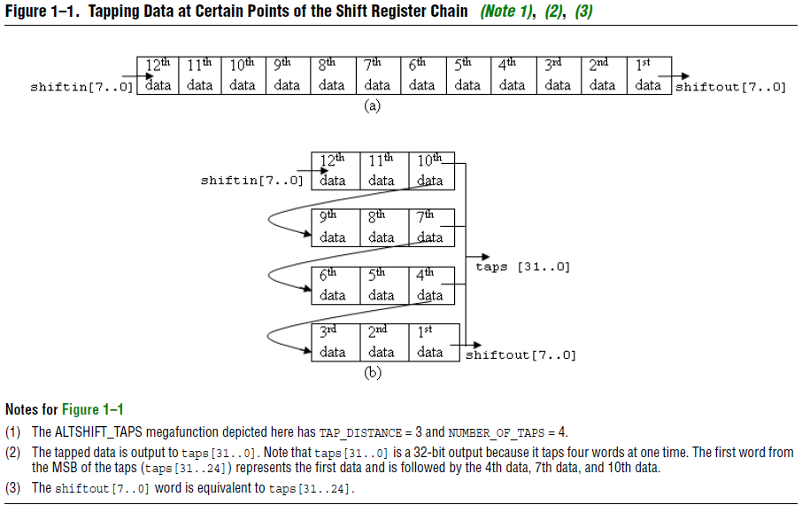
This example uses The altshift_taps megafunction to produce a shift register. You can specify multiple taps as output as shown below (from RAM-Based Shift Register Megafunction Users Guide). The example includes the altshift_taps module and a PLL. The shift register is set up with two taps, each of length=4. The read_data output is therefore delayed by 8 cycles and the taps[7:0] output is delayed by 4. The archive includes a signal tap module to probe the counter, the output data, and the taps output. Triggering the state machine on either edge of the memory clock works.