The MIDI specification requires for optical isolation on the input of the signal. Furthermore, the MIDI spec treats a signal high as a 0mA current source and a signal low as a 5mA current source. The final designed circuit is a modified version of that provided in the “MIDI Electrical Specification” and the “Arduino MIDI-in shield” Instructable. The circuit is shown below:
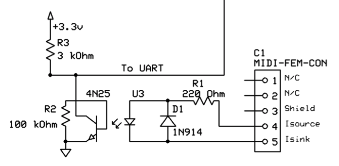
R1 is used to provide the necessary voltage drop for the optical isolator turn on voltage. R2 is used for biasing the transistor inside the optical isolator to have a higher response. We are operating the optical isolator in BJT-saturation and can model the transistor as a ground connected switch. To make the PIC32 micro controller able to read this switch, we use R3 as a pull-up resistor for the UART Rx line.
UART FIFO
On board the PIC32MX250128b, there is a 4-input FIFO buffer on the UART receive lines. This is nice because the when a MIDI message is received, it will queue in this buffer until it is read. A downfall of this buffer, however, it is only 4 inputs. This means that if more than 5 bytes are received before reading the UART, this buffer will overflow. The PIC32 has an interesting feature that prevents receiving anymore bytes on the UART bus until the overflow error is cleared. When MIDI sends a note on or off command, 3 bytes of data are actually sent. If multiple notes are played too close to each other or conflict with other MIDI messages, this buffer could easily overflow. In order to overcome this issue, we either need to implement a hardware buffer or a fast, interrupt based, software buffer. We caught this error too late in the game to implement this for our project, but a software buffer seems the most promising.
12-Bit DAC
For digital to analog conversion, we chose to use the MCP4822 12-Bit DAC from Microchip. We had used this chip in a prior lab and it worked quite well. Because all chips were to be soldered to perf-board, we wanted to leave the option for stereo effects open via software at a later point without changing hardware. This DAC has 2 channel output, so we soldered each channel to the Left and Right channels of a 3.5mm audio jack. The input data to the DAC was achieved using SPI bus 2 on the PIC32. (The TFT was used on SPI bus 1).
Microstick Socket
A requirement of the final project was to keep the Microstick II and/or the PIC32 not soldered directly to the board. We found that a 40pin DIP IC socket with 0.6” spacing between the pin rows fits the Microstick II perfectly. By using a 40pin header instead of a more appropriately sized 28 pin socket, we also had some extra socket locations that we turned into Vdd and ground rails for testing or prototyping. These extra pins would be removed if we switch to a more permanent board solution.
Project Enclosure
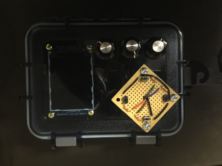
From the initial brainstorming of the project, one of our group’s goals all along was to have a finalized looking product at the end. We wanted something that looked more like an initial prototype design than an in progress test. We purchased a small waterproof enclosure from Walmart. On top of that box, we tried an initial layout by physically placing components. This initial layout is shown below: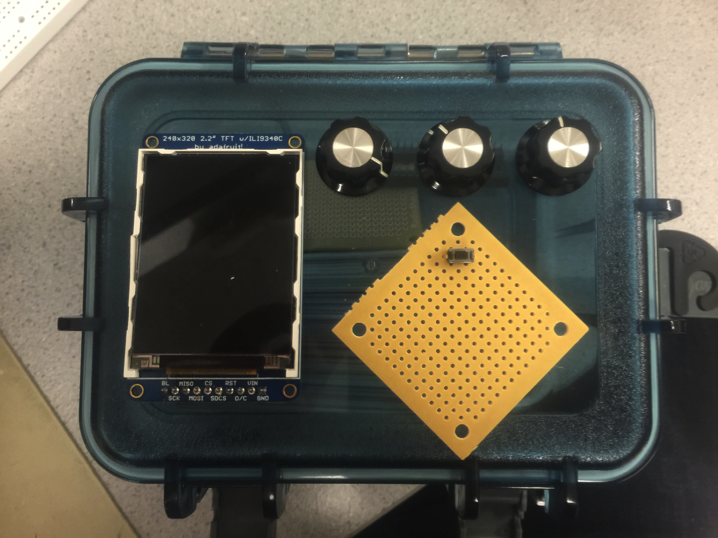
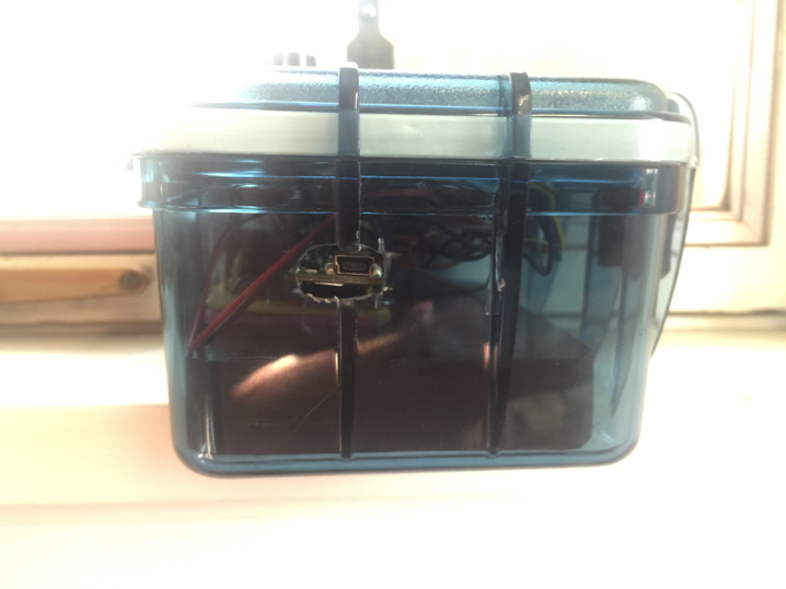
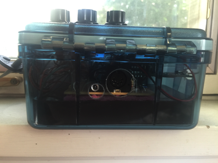
From this we began to solder connections to perf board, drilled holes in the case to mount potentiometers, the screen, and ports. On the top of the box, we ended up mounting the TFT display on the inside of the box, facing outward. Other than that, we matched the initial layout pretty closely to the final layout. Our final layout and port holes are shown in the images below: