![]()
![]()
![]()
![]()
![]()
![]()
![]()
![]()
![]()
![]()
![]()
![]()
|
Prototype Once the functional requirements of the board was identified (see overview), hardware schematics were drafted. The initial design consisted of 3 functional circuits, which are very close to the boards used on the existing PCB.
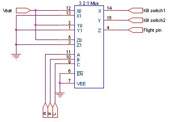
The circuit that simulates the the kill switch and flight pin is shown above. The design of this circuit is very straightforward: Power Board Connector B has GND, VBatt and select lines on it. When the Flight Pin select line is connected to VBatt and either one or both of the kill switches are connected to VBatt, the satellite will turn on. Since the select lines are inputs to Mosfet gates on the power board, there is little to no current draw and the use of the Multiplexer as shown in the above schematic makes sense. However, we did run into some voltage issues: The DIP package of the multiplexer that we used works correctly when sending 12V through it, while the SMT component will flake out, usually permanently at larger voltages. This caused severe inconsistencies during testing of our prototype and PCB circuitries. Unfortunately, we have determined this limitation ultimately keeps our maximum MUX voltages to around 3V for all circuits and prevents us from sending VBatt (12V) through to demonstrate integrated functionality of the Power Board and Diagnostics Board. This demonstration of proper functionality has further ramifications in other circuits as they too were prototyped with the DIP package and break in similar ways. This issue can be easily resolved with these higher voltage multiplexers. Unfortunately, our board does not have a compatible pin out with these components & can therefore should not be hooked up to the power board directly. Initially, the multiplexer was chosen because of its availability and cost. Our first choice was a MAXIM chip that ran off of any voltage between 5 and 36V and allowed for any value between Vcc+.5 and Vee - .5 to pass. This part was unavailable at the time and was a bit too expensive to use in each of the circuits as required.
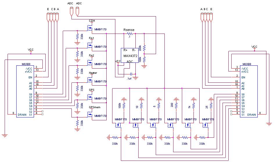
Once the circuit to test "power on" was created and tested, a regulator measurement circuit was created (above). The regulator expands in complexity compared to the Kill Switch & Flight Pin simulation circuit. This circuit uses 2 8:1 demuxes to allow the Diagnostics board to select one regulated input, pass the current through a common RSense resistor and Voltage divider and finally selecting which of 4 power resistor loads to use. The first MUX chooses the input to measure. The demultiplexer has 5V as a single input and 8 outputs that are connected to the gates of transistors (all of which have pull downs for when they are not being selected). This allows us to select which one transistor to turn on. The transistor that turns on, passes its input voltage from source to drain. Once through the transistor, the signal passes through a .1 Ohm sense resistor. A MAX4372 is used to measure the voltage on either side of the sense resistor, which then provides the ADC with a voltage that represents the current based on the knowledge that there was a .1 ohm resistor there. Once through the sense resistor, a voltage divider sends 1/3 of the voltage to the MCU to allow it to take measurements up to about 15V. At this point, another MUX is controlled by the MCU, which selects the appropriate power resistor to load the regulator signals with in the same way the first MUX selected the transistor. This design ensures that only one of the regulator outputs be loaded at a time. Additionally, when voltages are being read, the second mux is disabled to get an accurate voltage reading. This is consistent with the power test document as well as the projects goals. Simply selecting the appropriate regulator to load is not sufficient as they won't be on by default. To turn the circuits on, a voltage must be applied by the MCU to the select line going into the power board this voltage comes from PORTB.4-7 and PORTC.0-5. In future revisions, this may be removed due to the active effort to make the power board control its own hardware and depend on MCU communications rather than voltage levels, which will add reliability as well as reduce I/O requirements.
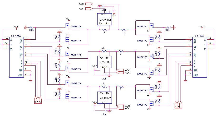
The torque coils test circuit is the most complicated of the 3 and we were prepared to see issues with it due to its bidirectional nature. This circuit is similar to the 8:1 MUX circuit. However, it uses 2:1 MUXes and is repeated 3 times (once for each axis). The select lines of the multiplexers are tied together. When a select line is asserted, one direction for the axis is selected on one side and the opposite direction is selected on the other. This effectively reverses the H-bridge bi directional effect and allow the current sensors to deal with just one direction of current. Unfortunately, we did not hook the MUX enable lines up to port pins for this circuit. Doing so would create a much more accurate Voltage reading as the last transistor essentially becomes an open circuit and the voltage divider is much more useful. There are various capacitors, resistors, crystals, headers, etc. that connect to the ZIF socket. If interested in recreating a 128L board, use the ExpressPCB file for reference. Please see PCB errors in Schematics. MEGA128 Port Assignments
PORT Designations: PCB Our project was laid out by hand in ExpressPCB. The layout took at least 75 hours combined. The board is relatively large, especially when compared to the power board. Fortunately, our careful layout paid off. Upon population of about 162 components, the MCU immediately worked, with the exception of a quirky & inconsistent Serial0 receive issue upon reset. Other errors were found, but largely the board layout was fine. PCB Features Include
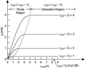
MCU Selection The processor itself supports dual serial communications and has 7 Ports. Aside from being free, these are the two main reasons for MCU selection. The dual serial ports connect to a MAX232 surface mount IC. Serial0 is accessible through the 9 Pin serial connector while Serial1 is accessible through either the second port or the power board MOLEX connector, which is set by a jumper. Hardware Design Issues Once populated, we ran into problems detecting voltages and current changes above around 3V. This was quickly found to be a transistor biasing problem. In order to detect voltage drops, our design requires us to operate in the triode region through 12V. However, due to the 3V restriction on Vgs due to the MUX limitation, we end up saturating early and the current becomes limited but this more to do with being on the wrong Vgs curve as opposed to being in the saturation regime. Since the transistors are not biased appropriately, they don't behave like an on off switch as intended, but this should become significantly better with a higher Vgs. If the same design is kept in the future, the following inequality must hold true: Vds < Vgs - Vtn
We have a good idea regarding a fix and many suggestions have been given to us, but they all require drastic hardware changes. The following are the best candidates thus far and will be considered for future revisions.
Another issue is the current is most likely being limited through the transistor at time, more testing should be done to correlate the amount of current drawn by this board, during manual power board testing and during flight operations.
|
|
Cornell University -
ECE 476 Final Project
Bryan
Doyle & Michael Austin - Spring 2005