Cornell University ECE4760
Inter-Integrated Circuit™ (I2C™)
PIC32MX250F128B
I2C on PIC32
I2C is a two-wire, synchronous bus designed to be cheap to implement on a single board. It is only moderately fast, usually lower than
400 KHz SCL baud rate. The bus electrical protocol (open drain, slew rate control) and logical protocol (start, restart, end) conditions
means that you must use the I2C hardware on the PIC32.
This page considers only single master systems, where the PIC32 is the
only master.
The following material may help in understanding I2C (simplified from Reference Manual chapter 24).
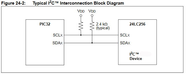
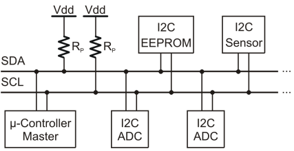
Figure 24-2 shows the conceptual layout of the cpu and a I2C connected peripherial.
Up to 128 peripherials may be on the same two wire bus, each with it's own address signalled on the bus.
Basics of I2C :
• The data bus is bi-directional and that external pullup resistors are required.
Internal pullups generally will not work because their effective resistance is too high.
During early stages of testing, you must scope SDA and SCL lines to check voltage levels!
Because the SDA and SCL lines are bidirectional, the output stages of the devices driving the
SDA and SCL lines must have an open drain
in order to perform the wired AND function of the bus.
• SCL is the clock for the bus, which is always generated by the bus master.
The clock baud rate may be set as high as 1 MHz, but most I2C peripherials will not accept >400 KHz.
• SDA is the bi-directional data line. All data, including peripherial addresses are carried by SDA.
• Each peripherial device has an address, usually specified on the device datasheet, but sometimes with hardware settable bits.
When a master wishes to initiate a data transfer, it first transmits the address of the
device that it wants to “talk” to. All devices “listen” to see if this is their address.
As part of this address, bit 0 specifies if the master wants to read from or write to the peripheral device.
• The peripherial device address may be fixed by the device manufacturer, set by logic levels on pins on the device,
or a combination of the two.
--
For example the SGS ST24/25x02 EEPROM has a hardwired 4 bit address (0b1010000) and three
pins to set another 3 bits of low order address. This means that no more than eight of these devices can be on one bus.
-- Another example is the Microchip 24LC256 EEPROM which has three address pins to set the address. But later in the data sheet
we find that the top four bits are set to the control code 0b1010000, which is essentially the same as the other EEPROM.
Bus Protocol:
• Data transfer may be initiated only when the bus is not busy
• During data transfer, the data line must remain stable whenever the SCLx clock line is high.
• Changes in the data line while the SCLx clock line is high will be interpreted as a Start or Stop condition.
Note that a stop/start condition may be generated on the same clock cycle. This is called a Restart. A restart allows the master
to continue to control a given peripherial with no break to allow another transfer to take control.
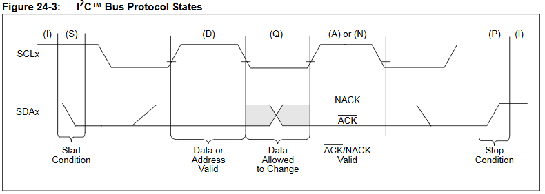
Refering to the image above:
• START DATA TRANSFER (S) After a bus Idle state, a high-to-low transition of the SDAx line while the clock (SCLx) is high determines a Start condition.
All data transfers must be preceded by a Start condition.
• STOP DATA TRANSFER (P) A low-to-high transition of the SDAx line while the clock (SCLx) is high determines a Stop condition.
All data transfers must end with a Stop condition.
• REPEATED START (not shown) A high-to-low transition of the SDAx line while the clock (SCLx) is high allows a Repeated Start condition when no STOP has occured.
Repeated Starts allow a master to change bus direction of addressed peripheral device without relinquishing control of the bus.
• DATA VALID (D) The state of the SDAx line represents valid data when, after a Start condition, the SDAx line is stable for the duration of the high period of the clock signal. There is one bit of data per SCLx clock.
• ACKNOWLEDGE (A) OR NOT ACKNOWLEDGE (N) All data byte transmissions must be Acknowledged ( ACK ) or Not Acknowledged (NACK) by the receiver.
The receiver will pull the SDAx line low for an ACK or release the SDAx line for a NACK.
The Acknowledge is a one-bit period using one SCLx clock.
• WAIT/DATA INVALID (Q) The data on the line must be changed during the low period of the clock signal.
Devices may also stretch the clock low time by asserting a low on the SCLx line, causing a wait on the bus.
• BUS IDLE (I) Both data and clock lines remain high at those times after a Stop condition and before a Start condition
Message Protocol Example:
The hardest part of getting i2c running with a new chip is understanding how the chip uses i2c to communicate. While the electrical protocol is standardized, the meaning of the payload of each transmitted byte depends entirely on the details of the chip. The message protocol depends on the specific peripherial device characteristics and is different for each different chip! Getting the protocol right for a new chip typically takes 10 to 40 hours of programming!
For the Microchip EEPROM mentioned above a typical memory read might be:
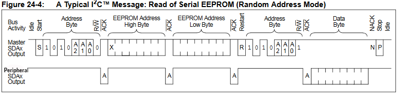
Refering to the image above:
• START MESSAGE Each message is initiated with a Start condition and terminated with a Stop condition.
The number of data bytes transferred between the Start and Stop conditions is determined by the master device.
As defined by the peripherial device protocol, the bytes of the message will have specific meaning, such as device address byte or data byte.
• ADDRESS DEVICE The first byte is the device address byte, which must be the first byte of any I2C message.
It contains a device address and a R/W bit in the low-order bit. Note that R/W=0 for this first address byte, indicating that the
master will be a transmitter and the device will be a receiver for the next bytes transfered.
• DEVICE ACKNOWLEDGE The receiving device is obliged to generate an Acknowledge signal, ACK , after the reception of each byte.
The master must generate an extra SCL clock which is associated with this Acknowledge bit.
• MASTER TRANSMIT The next two bytes, sent by the master to the memory device, are data bytes containing
the location of the requested EEPROM data byte. The memory must Acknowledge each of the data bytes.
This protocol is specified by the specific memory device data sheet and will be different for each different device.
• REPEATED START The memory now has the address information necessary to return the requested data byte to the master.
However, the R/ W bit from the first address byte (after the start) specified master transmission and device receive.
The bus must be switched for the memory device to send data to the master.
To perform this function without ending the message, the master sends a Repeat Start.
The Repeated Start is followed with a device address byte containing the same device address as before but
with the R/W=1 to indicate device transmission and master reception.
• DEVICE REPLY Now, the memory transmits the data byte by driving the SDA line,
while the master continues to originate clocks but does not drive its SDA line.
• MASTER ACKNOWLEDGE During reads, a master must terminate data requests to the peripheral by Not Acknowledging
(generating a “NACK”) on the last byte of the message. Data is “Acked” for each byte, except for the last byte.
• STOP MESSAGE The master sends a Stop to terminate the message and return the bus to an Idle state.
Programming I2C:
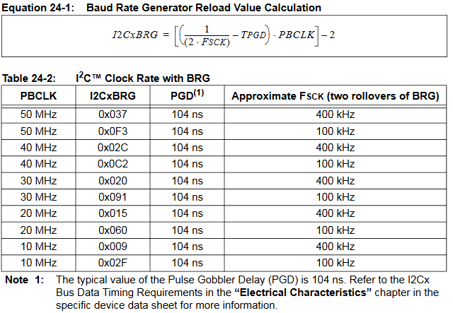
Refer also to PLIB manual section 16 Also refer to PLIB examples, particularly I2C master. Also you will need to set
up the I2C baud rate generator when you open the channel using OpenI2Cx(config, I2CxBRG)
There are some online resources to help with I2C coding.
-- i2c_helper.h by Stefan Karlsson seems to be the basis for several of the projects below.
-- This App note from Microship is for a different PIC, but describes the protocol well.
-- A microchip presentation on i2c.
4760 projects using i2c
-- The 2017 project 3DOF STEWART PLATFORM sets up I2C for the MPU6050 6-axis accelerometer/gyro
--
The 2017 project Far Infrared Thermal camera sets up I2C for a Lepton board.
-- The 2015 balancing robot project shows how to set up I2C for the Invensense MPU 6050 IMU.
Particularly, look at Appendix A, which defines a i2c_helper header to simplifiy the PLIB interface.
-- The 2015 Blimp-O project uses a MMA8451QR1 3-axis accelerometer an inlines all the code, but the
baud rate specification does not make sense. The hex eqivalent of 9600, 0x2580, happens to have the
correct lower bits to set the I2CxBRG to 0x80 which falls in a valid region.
-- An example from Northwestern Univ shows how to connect two PIC32s.
Copyright Cornell University
July 16, 2020