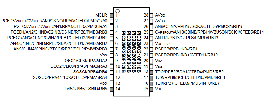
PIC32MX250 full pinout and signals from datasheet.
There is a more detailed explanation of i/o structure here.
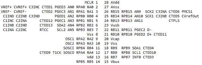
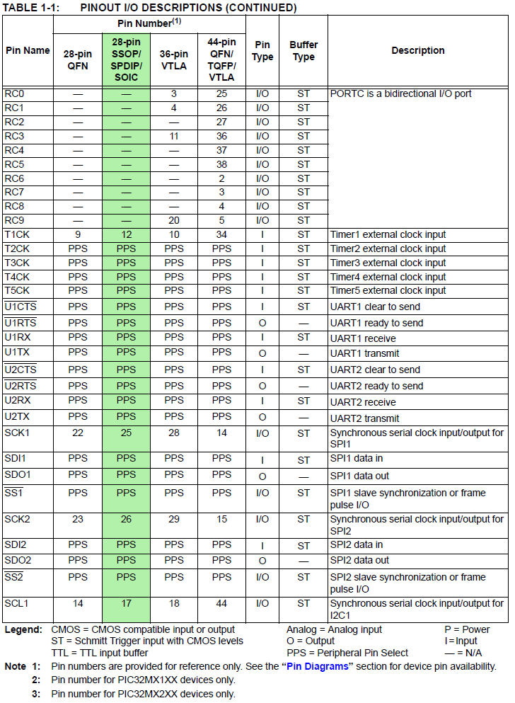
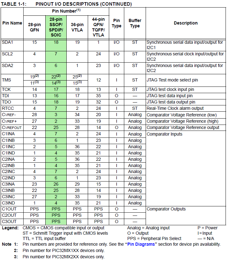
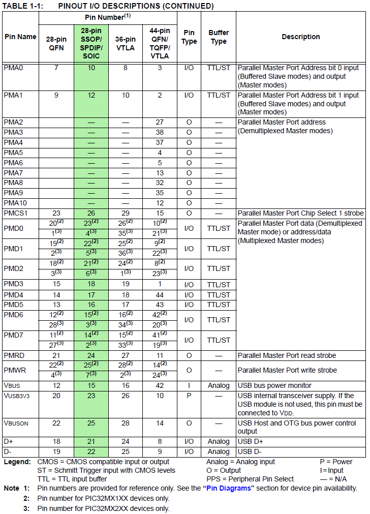
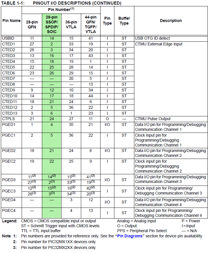
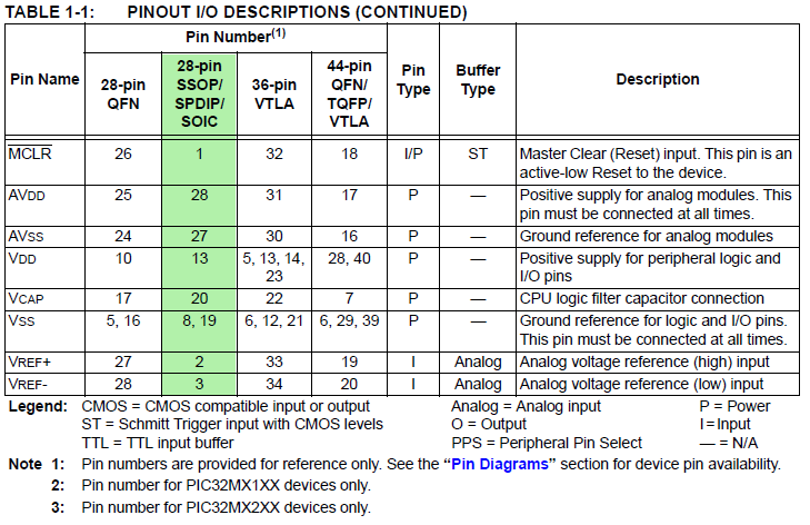
My slightly simplified version, organized so that humans can read it.
Click image for signal name definitions.
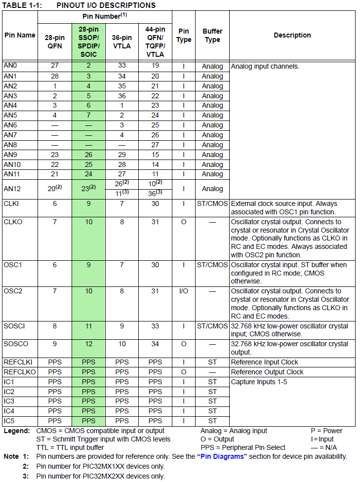
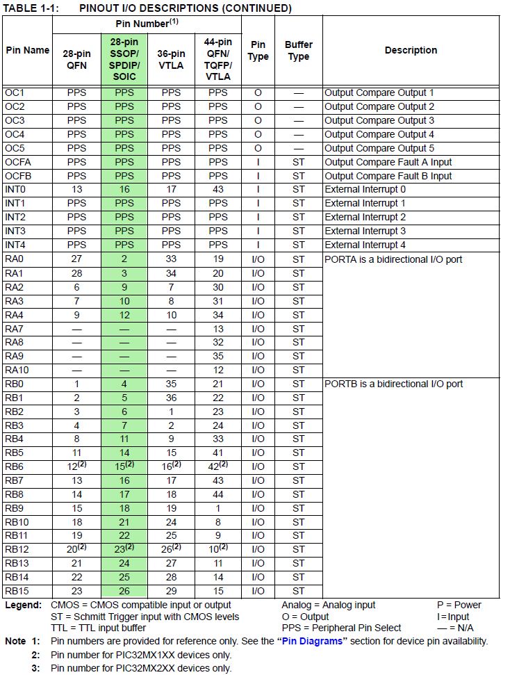
Signal Names==>Pins: 1, 2, 3, 4, 5, 6, 7 PDIP-specific signals highlighted in green
(for PPS see next tables)
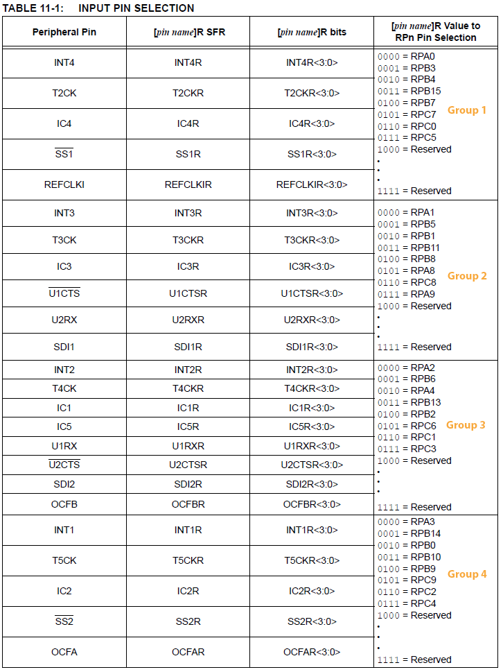
PPS redirects specific logical input/output signals to groups of i/o pins. For instance, one of the input capture inputs, IC1, can be routed to one of 8 different physical pins (see input table below). This feature helps with fitting designs onto the relatively few pins on the PDIP PIC32. Note that not all logical device signals can be PPS routed. For example, when an SPI channel is turned on, SCL1 and SCL2, the SPI clock lines are at fixed i/o pins 25 and 26 (RB14 and RB15). When a SPI channel is disabled, the respective clock pin can be used for general i/o.
Peripheral Pin Select (PPS) input table (from datasheet, but note added GROUP numbers)
--example: UART receive pin --- specify: PPS group, signal, logical pin name
PPSInput(2, U2RX, RPB11); //Assign U2RX to pin RPB11 -- Physical pin 22 on 28 PDIP
Note that the groups (1 to 4) are delimited by horzontal lines in the righthand column of the table.
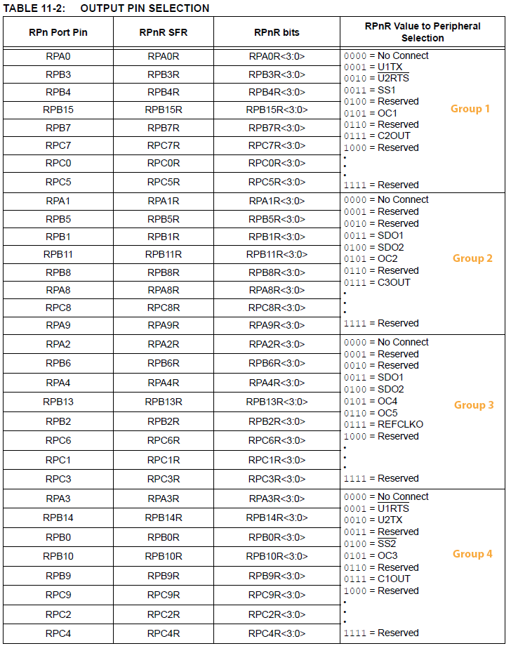
Peripheral Pin Select (PPS) output table (from datasheet, but note added GROUP numbers)
--example: UART transmit pin --- specify: PPS group, logical pin name, signal
PPSOutput(4, RPB10, U2TX); //Assign U2TX to pin RPB10 -- Physical pin 21 on 28 PDIP
Note that the groups (1 to 4) are delimited by horzontal lines in the righthand column of the table.
PIC32MX250 configuration options Nota bene! If certain functions seem to not work, check these!
JTAG enable overrides pins 13, 14, and 15
Primary oscillator enable overrides pins 9 and 10
Secondary oscillator enable overrudes pins 11 and 12
There are silicon errors in I2C implementation that affect other i/o pins and other functions.
READ the errata RA0 and RA1 and RB5 and RB6 may be affected.
Further Simplified PIC32MX250 pinout (many less used signals are not included)
---------------------------------------------------------------------------------------
MicrostickII pinout (of historical interest only)