Introduction
Learn about the project goals and high level description.
Spring 2019 Advanced Microcontroller Design Final Project
Our ECE 5760 Final Project uses the Terasic DE1-SoC's Cyclone V FPGA and Cortex-A9 cores to fully simulate a Xilinx XC6200 FPGA. We test the functionity of the hardware-simulated FPGA and experiment on its ability to discern between input frequences using a genetic algorithm. Our project follows on to research pioneered by Adrian Thompson in 1996. We discuss the practicality of Evolvable Hardware and challenges in implementation.
Learn about the project goals and high level description.
Learn about the specifics of the project. Dive into design implementation and challenges.
How did the project perform? What worked and what did not work?
Take a step back and evaluate the end result of the project in more general terms.
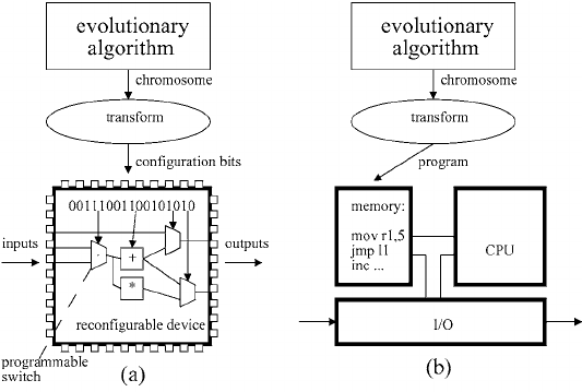
The goal of our project was to simulate an FPGA design on our system, to allow us to experiment with evolutionary hardware using a genetic algorithm. Inspired by Adrian Thompson's 1990s research on the subject, we decided to simulate the Xilinx FPGA he used in his research, giving us the ability to quickly re-program the device and view it's internal data stream without limitations of IO or encryption.
The original vision was to implement the simulated FPGA and use an evolutionary algorithm to solve the same problem Thompson set his sights on - the discrimination between two input frequencies, both significantly greater in period than the propogation time between input and output of the device.
The following disigns needed to be implemented in order for us to start these experiments:
This section consisted of designing the verilog system implementation of the Xilinx XC6200 FPGA on our Cyclone V device..
This section consisted of building a program to control the simulated FPGA and evaluate its performance, using a C program running on the Cortex-A9 Hard Processor System.
This project was ambitious and had many sections which all had to come together before testing. Although the field of Evolable Hardware has been around for slightly over two decades, it is still a youthful field showing promise in signal processing and other areas.

Description of the DE1-SoC hardware and configuration.

Review of Thompson's research and the methods and devices he used in his work.

Implemenation of a simulated XC6200 FPGA on our Cyclone V board.

Description of High Perfomance System configuration to program simulated FPGA and evaluate results.

Description of how we implemented a three-bit Adder to test the simulated FPGA.

An overview of the genetic algorithm we used in an attempt to converge on an evolved hardware system using our simulated FPGA.
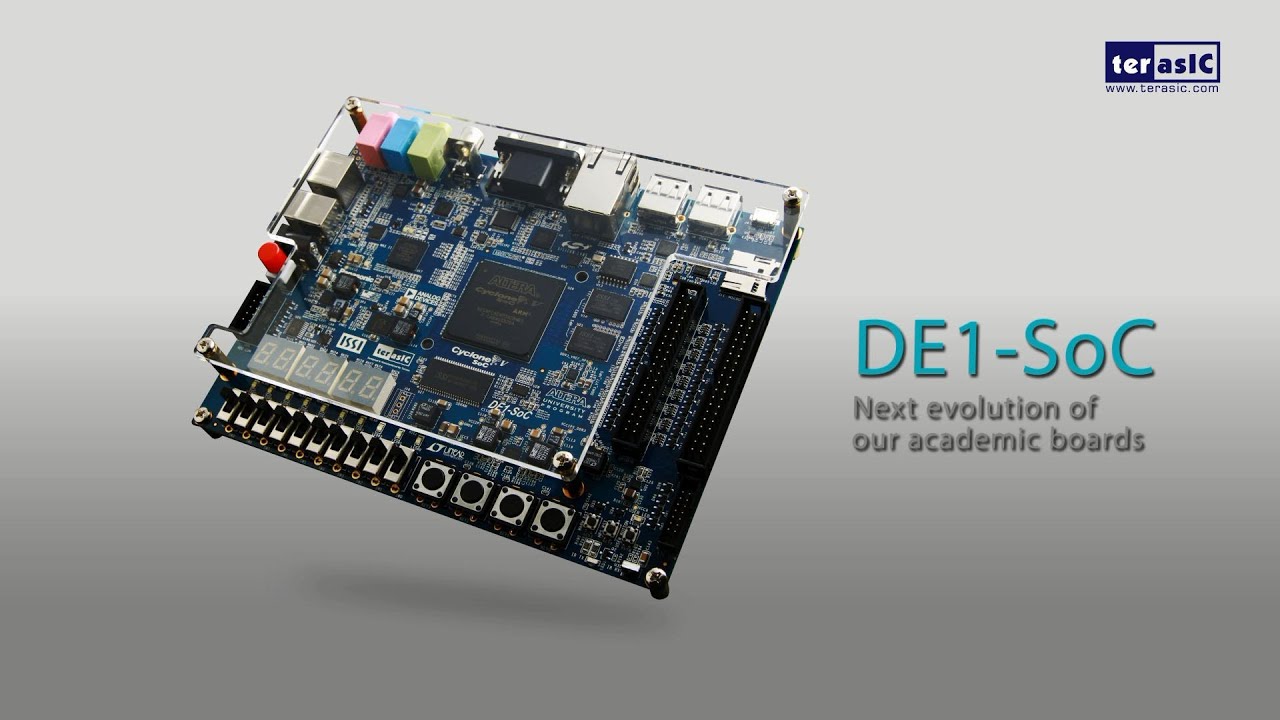
The DE1-SoC is a development board built around the Alterra 5CSEMA5F31C6 SoC. It provides an environment to design integrated projects with a Cyclone V Field Programmable Gate Array (FPGA) and a Cortex-A9 Hard Processor Systep (HPS). The FPGA is arranged to follow a Verilog HDL design, while the HPS runs Linux and any necessary code. The two devices in a single package share a high-bandwidth memory-mapped bus, and Qsys is used to design the bus backbone to allow the devices to interoperate seamlessly.
The system provides the following hardware features:
The Cyclone V has a fully encryped bitstream in its hardware design, making it very difficult to use for hardware evolution projects out of the box. We decided to simulate another FPGA on its hardware to get past this issue.
Dr. Adrian Thompson is a researcher in the Department of Informatics at the University of Sussex, and his experimentation in the mid 1990s represented some of science's first practical attempts in the field of hardware evolution. He used an early FPGA and a genetic algorithm to evolve the internal circuitry of his device, allowing it to breed and mutate in design until it was able to solve a fairly difficult problem. The concept is roughly analogous to Charles Darwin’s elegant principle of natural selection, which describes how individuals with the most advantageous traits are more likely to survive and reproduce. This process tends to preserve favorable characteristics by passing them to the survivors’ descendants, while simultaneously suppressing the spread of less-useful traits. It's a wild idea in hardware design, and his research inspired this project.
In 3500 generations of a genetic algorithm, Thompsons's FPGA was able to discriminate between two input signals in a completely unique way.
Abstract: `Intrinsic' Hardware Evolution is the use of articial evolution - such as a Genetic Algorithm - to design an electronic circuit automatically, where each fitness evaluation is the measurement of a circuit's performance when physically instantiated in a real reconfihgurable VLSI chip. This paper makes a detailed case-study of the first such application of evolution directly to the configguration of a Field Programmable Gate Array (FPGA). Evolution is allowed to explore beyond the scope of conventional design methods, resulting in a highly eficient circuit with a richer structure and dynamics and a greater respect for the natural properties of the implementation medium than is usual. The application is a simple, but not toy, problem: a tone-discrimination task. Practical details are considered throughout.
His paper has a striking title, but the content is even more exciting, with the most interesting aspects being the close entwinement between the found solution and the device phisics of his FPGA. When Thompson looked at the inner workings of the device, what he found inside was baffling. The chip was utilizing only thirty-seven of its one hundred logic gates, and most of them were arranged in a collection of feedback loops. Five individual logic cells were functionally disconnected from the rest— with no pathways that would allow them to influence the output— yet when the researcher disabled any one of them the chip lost its ability to discriminate the tones. Furthermore, the final program did not work reliably when it was loaded onto other FPGAs of the same type.
 The final evolved circuit
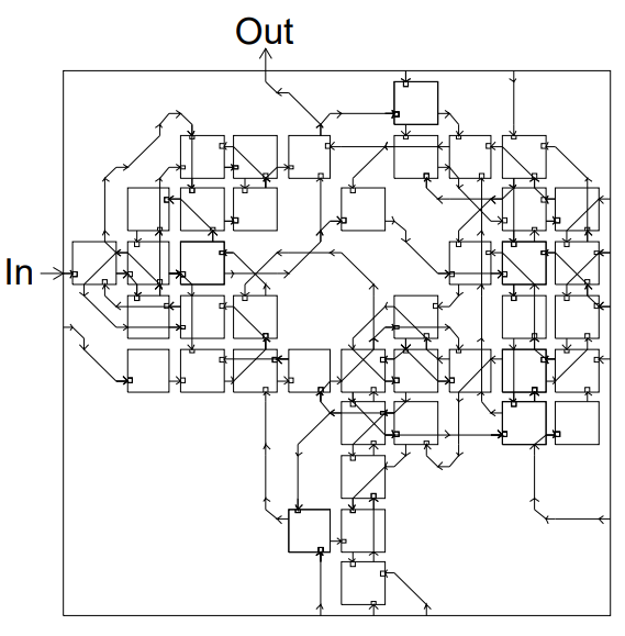 The circuit pruned down
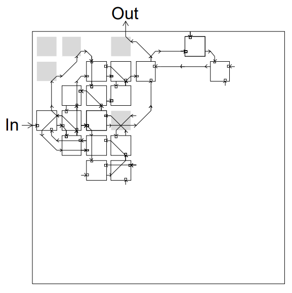 The functional part of the circuit
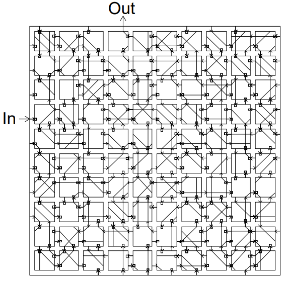
Thompson used the Xilinx XC6200 FPGA, which had a 10 x 10 array of cell blocks. This 100 logic gate arrangement is miniscule by today's standards, but the platform also came with some powerful functionality in it's ability to connect any cell directly to it's neighbor on any side, or to pass through signals.
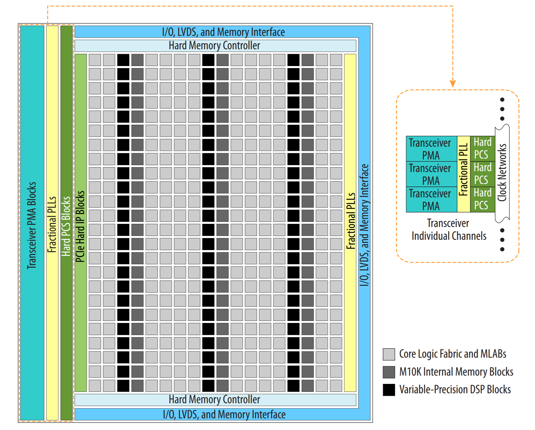
The internal design of our FPGA is a set of many Adaptive Logic Modules (ALMs), which are the building blocks of the FPGA design. However, the ALMs used in the Cyclone V are focused on providing digital design features helpful in synthesising common digital logic, and provide a lot less flexibility per elemement than the functional units that made up Thompson's XC6200 device. Our FPGA holds 85k logic elements (ALMs) also holds M10K and MLAB memory blocks. The general overview can be seen above.
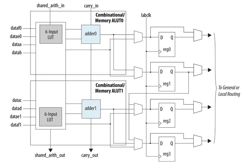 Cyclone V ALM
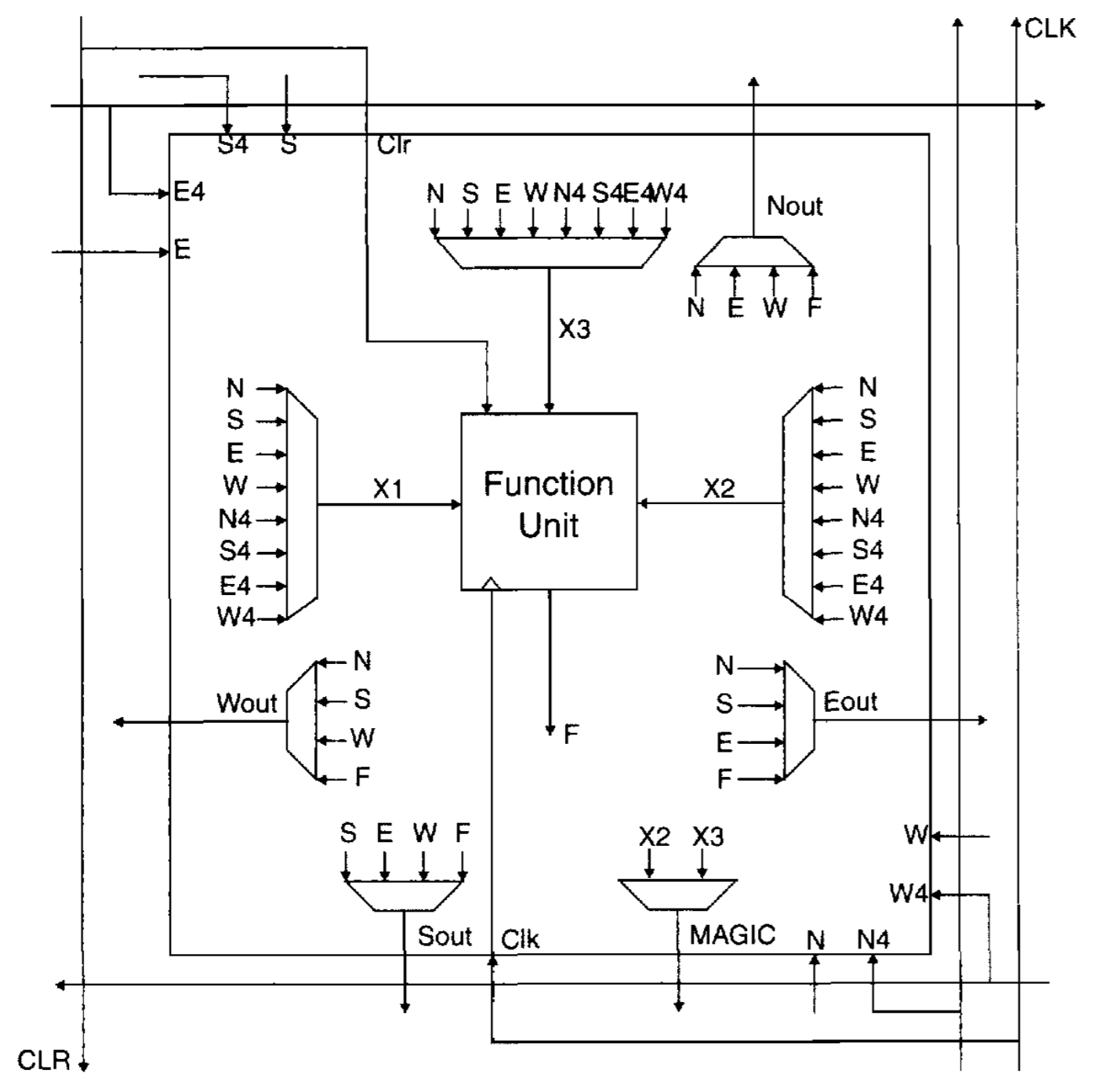 XC600 Cell
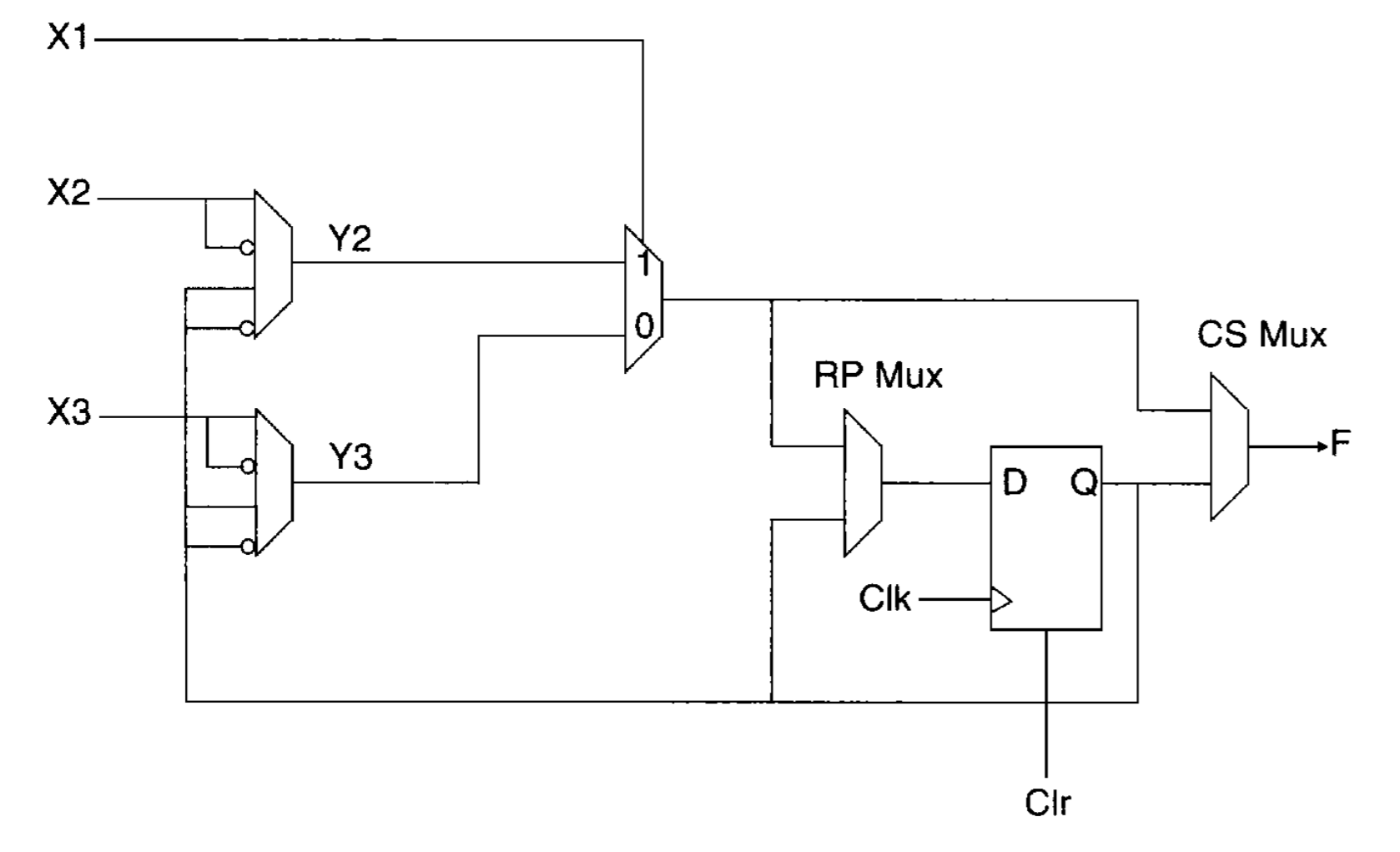 XC6200 Functional Unit
The Cyclone V ALM consists of a eight inputs to a set of look up tables and adders, and some digital logic and four registers. When compared with the XC6200 design, we have far less control in how each logic element is connected to its nearest neighbor, making the type of localized design needed for this project difficult or impossible. Instead of trying to create genetically modify the design of our hard FPGA, we decided to simulate the XC6200 design on our board.
The XC6200 logic cell can be seen above, featuring digital connections to each of its nearest neighbors, designed by the cardinal directions NSEW. It can also pass through signals to other cells further out. The functional unit and cell interconnections are implemented in our FPGA in system verilog. Although much less efficient in usage of logic elements, we are able to fit a full 10 x 10 array of XC6200 simulated elements on our DE1-SoC's FPGA.
A full listing of implementation code can be found in the appendix.
One large benefit of developing an FPGA on top of the preexisting one is having complete access to the bitstream that runs programs on the hardware. As the FPGA is able to be programmed with the upload of a 4032 bit vector, theoretically any combination of those 4032 bits can produce a functional FPGA layout. Compiling a program for even a very basic task is a very tedious process however, as we saw in the hand-compiling of one such program to produce a 3-bit adder with carry-out.

The HPS runs a C program to control the simulated FPGA and genetic algorithm. More information can be seen in the Genetic Algorithm section.
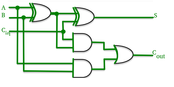 A Carry Look-Ahead Adder
 Adder Output
In order to implement an adder on the simulated fpga, we had to generate the structure of the device entirely by hand. Normally synthesis of such a design is handled by the Quartus solver, but we had no ability to write our own synthesis solver for the simulated XC2600.
Instead, Ryan drew out the required interconnecteds on the whiteboard and wrote the 4032 bit vector almost intirely by hand. He acheived this by studying the structure of the bitstream, carefully writing values to specify connections, and then flipping the rows and converting the output to a single hex vector.
// row 0 000100 000 000 000 xx 01 xx 01 000100 000 000 000 10 00 01 xx 000100 000 000 000 00 xx 10 xx 000100 000 000 000 xx xx xx xx // row 1 000100 000 000 000 xx xx 10 01 000100 010 010 000 01 00 11 xx 000101 000 011 000 00 11 xx xx 000101 011 001 001 xx 11 xx xx // row 2 000100 000 000 000 xx 00 xx xx 000100 011 011 000 xx 00 10 11 000101 001 011 001 xx 11 xx xx 000100 000 000 000 xx xx xx 10 // row 3 000100 000 000 000 xx xx xx xx 000100 000 000 000 xx 00 xx xx 000100 000 000 000 xx xx xx 10 000100 000 000 000 xx xx xx xx
000100 000 000 000 10 01 00 01 000100 000 000 000 10 00 01 00 000100 000 000 000 00 10 10 00 000100 000 000 000 10 10 00 00 000100 000 000 000 10 10 10 01 000100 010 010 000 01 00 11 00 000101 000 011 000 00 11 00 00 000101 011 001 001 10 11 00 00 000100 000 000 000 10 00 00 00 000100 011 011 000 10 00 10 11 000101 001 011 001 10 11 00 00 000100 000 000 000 10 10 00 10 000100 000 000 000 10 10 00 00 000100 000 000 000 10 00 00 00 000100 000 000 000 10 10 00 10 000100 000 000 000 10 10 00 00
00000000000000000000100140200280400500800a0100140200280400500800a0100140200280400500800a0 100140200280400500800a000000000000000000000100140200280400500800a0100140200280400500800a01 00140200280400500800a0100140200280400500800a000000000000000000000100140200280400500800a01 00140200280400500800a0100140200280400500800a0100140200280400500800a00000000000000000000010 0140200280400500800a0100140200280400500800a0100140200280400500800a0100140200280400500800a 000000000000000000000100140200280400500800a0100140200280400500800a0100140200280400500800a0 100140200280400500800a000000000000000000000100140200280400500800a0100140200280400500800a0 100140200280400500800a0100140200280400500800a000000000000000000000100140200288400400800a01 001442966c046c458800801593602860c0448260800a91001402000a040042080091000000000000000000001 00140200288400400800a01001442966c046c458800801593602860c0448260800a91001402000a04004208009 100000000000000000000100140200288400400800a01001442966c046c458800801593602860c0448260800a 91001402000a04004208009
Overall, though tedious to implement, this usage of the simulated FPGA confirmed it's functionality and ability to be defined by our software.
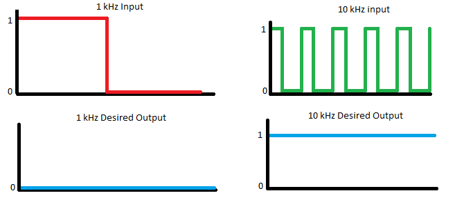
One way to generate a program that will produce an required output is to run a genetic algorithm on the possible 4032-bit vectors of the simulated fpga, with survival being biased towards the programs that produce the most accurate output corresponding to the output we desire. Depending on the heuristic used, this process can take many thousands, or even millions, of generations to produce a program with a decent enough fitness to be used generally for any input, and produce the expected output desired. For relative simplicity, we will build a genetic algorithm on our FPGA that attempts to classify two types of input, a 1 kHz square wave, and a 10 kHz square wave.
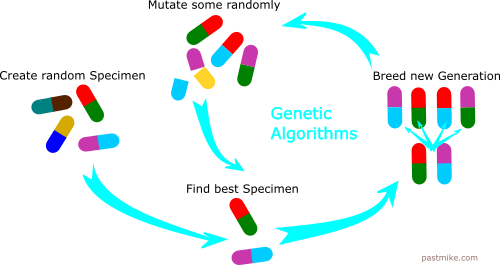
A genetic algorithm is a program that breeds and mutates models until eventually reaching a near optimal solution. It works very diffirently from most other machine learning algorithms. Here is a brief overview of our program:
Here, we run the program controlling this process whilst communicating with the FPGA over the proprietary AXI bus to swap inputs and outputs between the two systems.
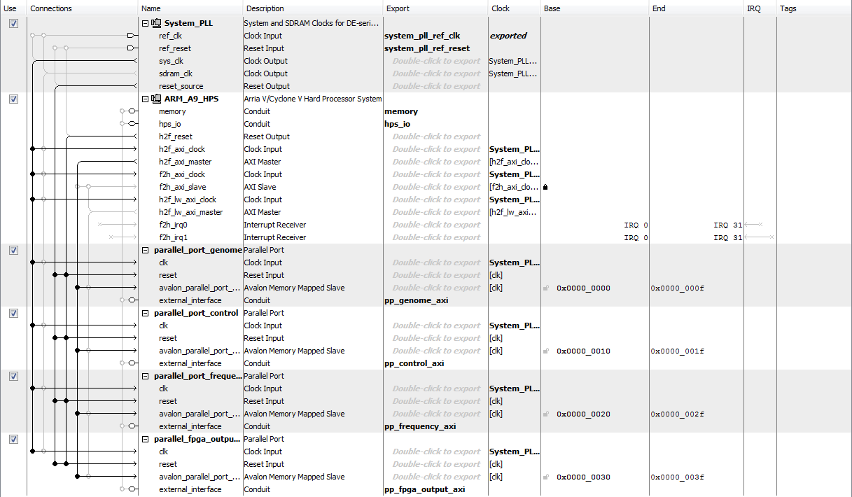
We first initialize a random population of 128 genomes, each just a randomly generated 4032 bit value that will participate in the genetic process. We then define the 4 Parallel IO ports that will communicate all data between the FPGA and HPS. These are instantiated in the Qsys platform designer (shown below) as slaves to the HPS.
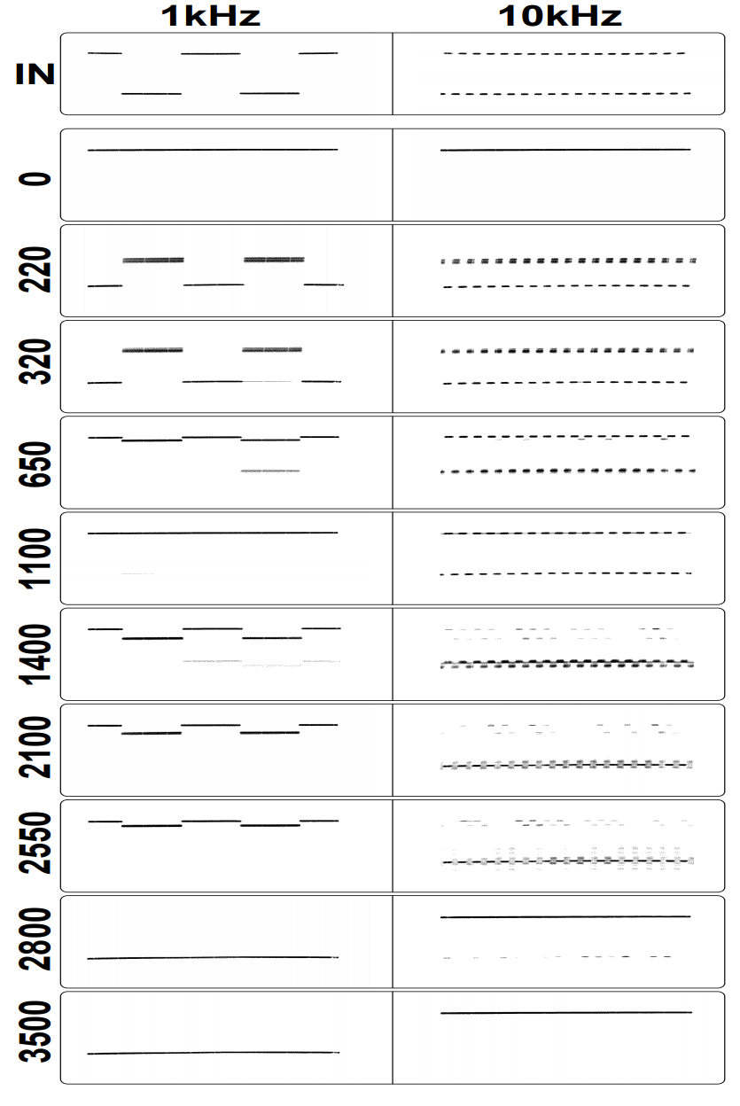
The first of these, parallel_port_genome, has a 32-bit data width which will upload the 4032 bit genome, over 126 iterations, to the custom FPGA. Each 32-bit word of this genome is triggered to be uploaded on the positive edge of the next parallel port (1-bit wide), aptly named parallel_port_control. Once this signal is dropped again, the next 32-bit word of the genome is ready to be uploaded. As soon as this program has completed being uploaded, the next parallel port, parallel_port_frequency (1-bit), is set low. Extra logic included in the top module of our Verilog design reads the value of this signal, and inputs either a low (1 kHz) or high (10 kHz) square wave to the custom FPGA. Just after this is set low, a timer runs for 50 milliseconds to allow the output behaviour to normalize. This value is picked somewhat arbitrarily, though is high enough that it allows most generated logic to produce an output corresponding to whatever input we feed it. The output value produced by the FPGA is then sampled 200 times, at a 100 kHz frequency. We chose this sample rate to allow a fine-grained sample range that takes into account the oscillating input value given by square waves. We expect that many random programs will change their output when that input oscillates, so it makes sense to sample outputs for both halves of that wave. With our chosen frequency, we are able to take 100 samples of both the peak and trough in the 1kHz square wave. This same process is repeated after setting parallel_port_frequency high.
Once all samples of the FPGA’s output are taken for each genome in the population, we must evaluate the fitness of each genome in this generation. We evaluate the fitness of a genome using a very simple fitness model. For just one frequency, the correctness of the FPGA’s output can be measured as the fraction of samples taken (for that frequency) which give the correct output.
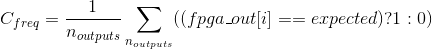
Keeping in mind that we would like the fitness value of each genome to reflect its accuracy for both the high and low frequencies at the same time, we find that the product of the value of C_freq for both the low and high frequencies, will only be large if both frequencies have high fitness. As such, we choose this for our fitness calculation.

Using the calculated fitness values, the next generation of genomes is produced. The top 20% of genomes (by fitness) move on with no effect on their data. The bottom 80% however, become subject to random mutations and crossing-over. Each of these genetic effects has only a 10% chance of affecting any given genome. Mutations in the context of the 4032-bit genomes, are the random flipping of a random bit in the genome. Cross-overs on the other hand affect two genomes at a time. Should one undergo that process, it will swap an entire, randomly chosen, 32-bit word with another, also randomly chosen, genome.
The entire process then starts over, for another generation. Lastly, we output the genome of the most-fit individual to a text file every 1000 generations, so that we have the exact bit vector that gives us the best 1kHz / 10khz classifier as determined by the algorithm after many iterations.
The simulated FPGA works almost exactly like the original XC6200 device, except that we are able to instantly re-program it and peer into it's inner workings at any time.
The Adder works as expected on the simulated FPGA, a strong data point towards Ryan's success as a manual FPGA solver.
Our genetic algorithm running on the HPS was able to successfully program and control the simulated FPGA, feed test signals into the system, and evaluate the fitness of each design. However after a day of computation and about 3,000 cycles of the algorithm, none of the mutations tested were able to discern between the two input signals. More testing is needed to either improve the speed of fitness evaluation, or otherwise modify the algorithm to get it to converge on a working solution to the problem.

The initial goal of the project was quite ambitious. While the final result did not demonstrate truly autonomous flight, I did manage to control a drone using an onboard PIC32 microcontroller. This really is the hardest part of the goal. Once I am able to control the drone, it is only a matter of sending the proper control signals.
Some portions of this project were adapted from existing code. For the GPS and magnetometer, my code was based on Adafruit libraries. The corresponding code has been linked and referenced accordingly. In addition to this, Betaflight was used to configure the drone's flight controller. Betaflight is open source software and also has bee linked in the appendix.
There are no legal considerations for this project as far as I know.
In designing and building this project I kept in mind the IEEE Code of Ethics to ensure that all users would be safe from harm. Drones are not the safest devices and can often behave sporadically. Especially when attempting to add autonomous flight. Becuase of this, I made sure to add a reliable killswitch. Arming and disarming a drone using a transmitter is the standard way to do this, and it provided a consistent and safe way to shut off the drone. When testing the drone flight, I made sure I was in a clear area and away from people. Any people around my area had to know about the drone prior to my testing.

This video shows our initial project demo in the ECE 5760 Lab.

The group approves this report for inclusion on the course website.
The group approves the video for inclusion on the course youtube channel.