Cornell University ECE4760
Direct Memory Access computing machine
RP2040
DMA on RP2040
DMA uses memory controllers separate from the CPU to accelerate data movment between memory locations, or between peripherials and memory. The RP2040 has 12 DMA channels which can stream an agregate of over 100 megabytes/sec without affecting CPU performance, in many cases. There are a huge number of options available to set up a DMA transfer. You can think of a DMA channel controller as a separate, programmable, processor with the main job of moving data. Memory on the rp2040 is arranged as a bus matrix with separate memory bus control masters for each ARM core and for the DMA system, and several memory bus targets accessed by the masters. Each bus target can be accessed on each machine cycle.
Here we use the DMA subsystem to produce a complete computing system, independent of the main ARM cpus. The DMA machine makes use of memory-copy ability, transport_triggered operations, and self-modifying code. The code consists of a sequence of DMA block descriptors stored in an array. The implemented operations are Turing Complete. About 8 million DMA blocks/second can be fetched/executed. There is a history of using only memory-moves to build a general cpu. In 2013 Stephen Dolan published x86 mov is Turing-Complete describing an example of a one-opcode machine. The paper Run-DMA by Michael Rushanan and Stephen Checkoway shows how to do this with one version (Raspbery Pi 2) of ARM DMA. The DMA system on the RP2040 has more transport-triggered functions and is a little easier to build. Joseph Primmer and I built a DMA processor using the Microchip PIC32 DMA system. Addition and branching had to be based on table-lookup. See DMA Weird machine.
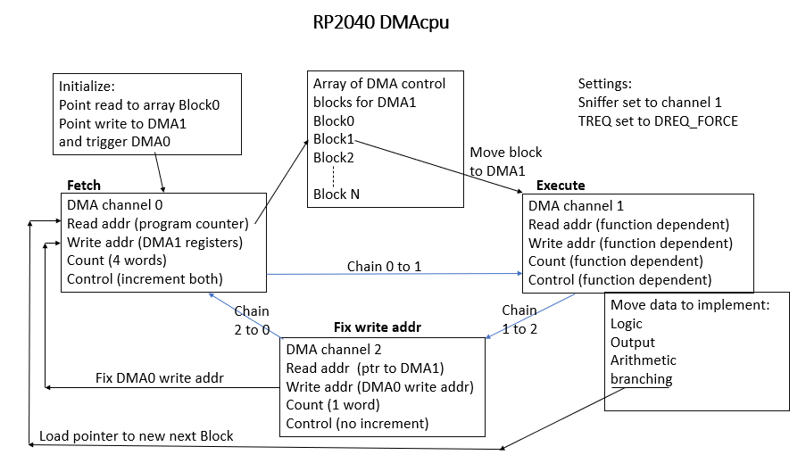
The DMAcpu
The DMA machine is a fetch-execute cpu where the fetch function is done by one DMA channel, which loads DMA control block images from RAM into another (execute) DMA channel. The 'program' which is loaded consists of a carefully crafted series of DMA control blocks which together act as a general purpose computer. By using DMA1 blocks to modify following DMA1 control block images in the array, just before they are transfered to the hardware DMA1 control registers, we can perform addition, increments, conditional jumps, and/or/not logic operations, and any other operations required. The design is made easier by several transport- triggered actions in the DMA subsystem. These include an adder in the 'channel sniffer' and atomic SET/CLEAR/XOR write functions on all SFRs. The basic fetch/execute machine uses the channel DMA0 read address as a program counter. Every fetch that occurs leaves the read address pointing to the next block location. DMA0 reads the next block from the RAM array and copies it to the DMA1 channel hardware control registers, then chains to the newly loaded DMA1 channel. The DMA1 channel performs whatever daata move is specified, then chains to DMA2. DMA2 resets the DMA0 write_address to point to DMA1 control registers. Program branching is implemented by using DMA1 to load a new DMA0 read address to the DMA0 control registers. Writing a program of DMA blocks is very much like programming in some strange assembly language for a machine with one accumulator register and only memory-to-accumulator operations.
The following diagram is an attempt to summarize all this madness.
Black arrows are data flow. Blue arrows represent chaining between channels.
The control block array is just an array of ints that are read by DMA0 in sets of four.
In addition to a straight copy operation, there are a few transport-triggered operations in the RP2040 DMA system which happen as a side effect of reading or writing a specific address:
The programming process has to map these unusual primitive operations into familiar mathematical and logical operations, and some form of conditional branch or jump. The sniffer add operation and the bitwise SFR operations means we can directly implement these functions.
But remember that every basic operation is just a data move.
For add a sequence of DMA blocks could be:
For shift-left we just do an ADD of a variable to itself (multiply by two).
For a logic operation (OR, AND, XOR, etc):
For subtract of (A-B) we have to explicitly compute the 2's complement negative of B:
For a shift-right the process is much more annoying. A right-shift is a bit-reversed left-shift :
An unconditional jump is easy.
One step: move the jump target address to the DMA0 hadware read address control word.
The hardest operation to get right is a conditional jump. Every jump condition (e.g. jump on negative number) must be converted into an absolute address and all data possibilities (e.g. positive, zero, negative) MUST JUMP! This is because the last step of setting up the conditional jump is to push data to the DMA0 hardware. This weird constraint means that jump conditions need to be converted to small integers representing block addresses. I will outline the jump-on-negative-number-in-variable scheme.
Simplifying Programming with DMAasm
It gets tedious to build programs by building DMA control structures. One solution is to package up one or more channel definitions into macros with better notation and more intuitive names. What I have come up with so far is in the table below. The latest program in the list below will have implementations. Each of the macros in the table below resolves to one or more sequential DMA control structures that make the DMAcpu look like a 1980's style, single accumulator, memory-to-ALU, architecture. The transport-triggered functions of the DMA sniffer register make up most of the ALU. Most of the DMAasm statments execute in about 125 nSec (8 million/sec), but a vector add or a multiply can be much slower, on the order of 100 adds/uSec. Multiplying by 256 therefore costs over 2 uSec. Shift-right by more than one bit uses the same add mechanism and can be slower.
| DMAcpu macro | Use and function |
|---|---|
| nop() | You guessed it! Skips one fetch/execute cycle. |
gpio_out(gpio_num, state)
|
Sets or clears one gpio pin given by gpio_num. The state is a variable which evaluates to a valid control word, e.g. int pin_hi = 0x3300 ;
int pin_lo = 0x3200 ;
|
load_sniff(var_name)
|
Moves one 32-bit value from memory to the sniff_data register |
store_sniff(var_name)
|
Stores one 32-bit value back to memory from sniff_data |
store_sniff_bitrev(var_name)
|
The sniff_data register has the ability to bit-reverse a number as it is being stored. This is occasionally useful, e.g. for the right-shift function |
move(source, destination, count, width, source_inc, dest_inc)
|
Move count items of bit-width width from source to destination. width must be DMA_SIZE_32 or DMA_SIZE_16 or DMA_SIZE_8
source_inc must have value var_read or array_read dest_inc must have value var_write or array_write If you move an array the source should be array_name[0] |
move_bswap(source, destination, count, width
|
Move count items of bit-width width from source to destination width must be DMA_SIZE_32 or DMA_SIZE_16 or DMA_SIZE_8
If you move an array the source should be array_name[0] |
set_sniff_CRC32()
|
sets the sniffer enable function to perform CRC32 on data passing through it, using the current sniffer_data value as seed. |
set_sniff_add()
|
sets the sniffer enable function to perform an cumulative add on data passing through it |
crc32_sniff(var_name, count)
|
Do the actual crc32 operation, taking count data items from var_name sniffer must be set to CSC32 |
add_sniff(var_name, count, source_inc)
|
Do the actual cumulastive add operation, taking count data items from var_name. This is a vector add. |
neg_sniff()
|
Take the 2's complement of sniff_data |
inv_sniff()
|
Take the logical not of each bit of sniff_data |
clr_sniff(mask)
set_sniff(mask)
xor_sniff(mask)
|
Low-level SFR direct write functions in which the mask to indicates which bits to change. |
or_sniff(var_name)
|
Logical OR of var_name into the sniffer |
and_sniff(var_name)
|
Logical AND of var_name into the sniffer |
shift_left_sniff()
|
One bit shift left |
logical_shift_right_sniff() |
One, 4, or 8 bit bit shift right - logical |
arith_shift_right_sniff()
|
One bit shift right - arithmetic |
mult_sniff(constant)
mult_sniff_var(var_name) |
Multiply by a LITERAL constant.
multiply ONLY by relative small, CONSTANT, positive ints. e.g. 4 or 20, but NOT 1000000
----- Mult by a variable, but remember that this is done by repeated addition and is slower for bigger numbers. |
jump(block_addr)
|
Unconditional jump to
block_addr which must be an int* variable assigned to an address, usually using something like
label(extra_pulse_addr)
|
jump_neg(block_addr_neg, block_addr_not_neg)
|
conditional jump
jump to two diferent locations on EITHER negative or positive/zero
the argument adressses MUST be int* variables with block addresses |
pacer(dreq)
|
Exection pacer. This just waits for the next DREQ event. If the event is a DMA clock tick then timer must be one of DREQ_DMA_TIMER0, DREQ_DMA_TIMER1, DREQ_DMA_TIMER2, or DREQ_DMA_TIMER3
And the timer must be set up. |
| label(label_name) | The label_name variable is assigned the address of the current block. Used for specifying jump and function addresses. The variable must be an int* |
jump_link(function_addr)
jump_return()
|
Jump to the specified address, and store a return address in the link register. Return from the function to the address in the link register. |
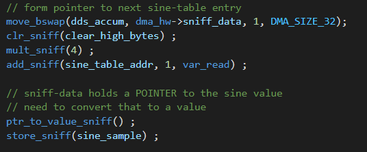
| ptr_to_value_sniff() | This macro is used to dereference a pointer contained in the sniff_data register and return the value to sniff_data. Useful for converting array addresses into data. |
The programs below are in blog-style reverse time order, newest stuff at the top.
The following program list is in time-order.
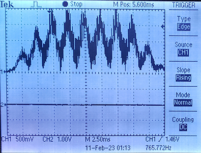
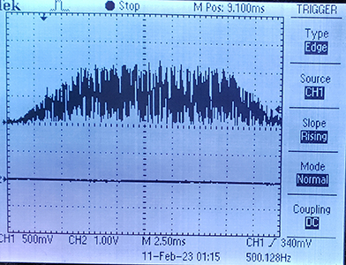
DMAasm noise+tone burst. (10feb2023)
The DMA program generates noise samples and DDS samples at 40KHz sample rate, sums them, then AM modulates into a burst. The main C program sets up the DMA program, generates a seed for the DMA rnadom number generator, then drops into a serial thread that prompts for sine wave frequency, burst duration, burst repeat time, and relative noise amplitude.
The images show a 400 Hz sine wave with medium noise, and just noise with no sine wave.
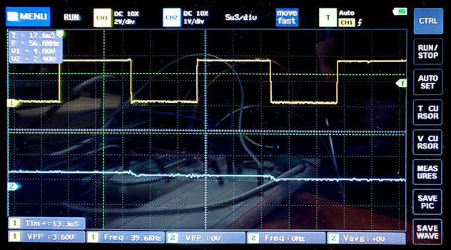
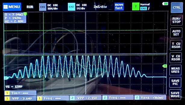
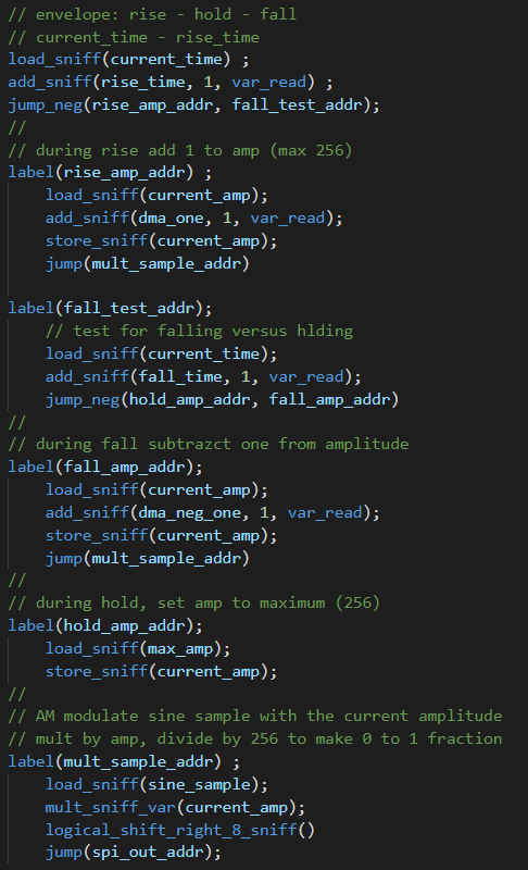
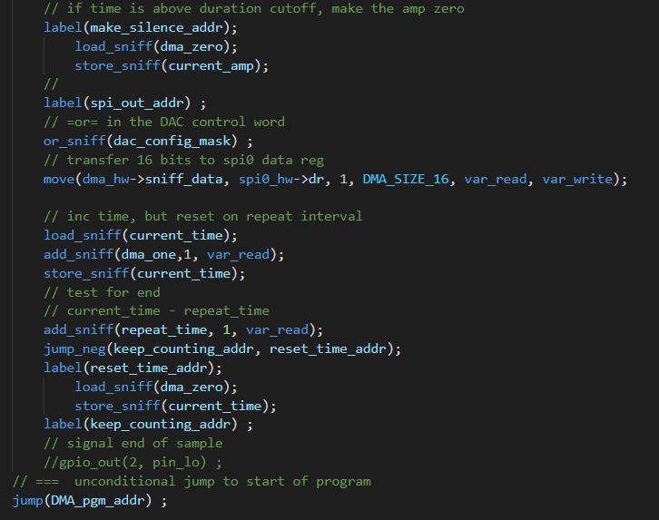
DMAasm tone-burst using DDS and amplitude envelope. (3feb2023)
This example tests many features of the DMAasm, while have a strict timing deadline of 40 KHz sample rate. The 88 DMA blocks generated by the assembler execute in between 5 and 13 uSec, well within the deadline time of 25 uSec.
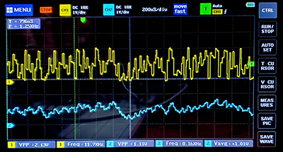
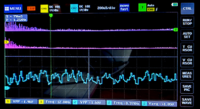
The tone bursts sound clean and glitch-free. Three code snippets show how the DMAasm is written. The first snippet is the DDS algorithm which increments the phase accumulator and gets a sine sample from a table. The second shows how the amplitude envelope is computing. The envelope is just a linear rise, constant, then linear fall. The third snippet shows the SPI output and undate of the burst timer. Two images show the DMAasm timing and a 1KHz burst. The sample compute duration (pulse-high) is approximately the longest sample execution time when the inefficient multiplies dominate the timing. There is exactly 25 uSec between pulses, set by the DMA pacing timer3. You can see the small steps in the output waveform as the DAC updates the voltage at the end of each pulse. It appears that the settling time of the DAC is <1 uSec.
DMAasm -- test of multiply, looping, subroutines (1feb2023)
The
program just asks for two two test values and a loop increment maximum. It produces a pulse train and some printed numerical results. The pulse train depends on the loop maximum and the sign of the first test value.
DMAasm -- Using memonic macros to make DMA programming a little easier (23jan2023)
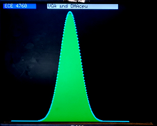
After writing a few programs, the most useful repeated constructions became more obvious and suggested that it should be possible to make easier to use macros which generate the DMAcpu program consisting of a list of blocks. As always, moving to a higher level means a little inefficiency, but it seems to be worth it. Each of the macros in the table below generates one or more sequential DMA control structures that make the DMAcpu look like a 1980's style, single accumulator, memory-to-ALU, architecture. The transport-triggered functions of the DMA sniffer register make up most of the ALU. The test program just exercises each of the DMAasm instructions, uses a serial thread to enter two test values and print results, and displays a normal distribution on the VGA to test the CRC32 code. GPIO2 is toggled. The pacing timer is set to 50 KHz. Entering a negative number at the serial command line for the first test value will exercise the conditional jump. There is support for a single-level of suboutine call (no stack).
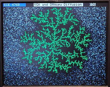
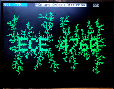
DMAcpu and DLA, with refined random number generation. (13jan2023)
DLA runs for 100s of millions random number evaluations, rather than the 100s of thousands used to generate the distributions in projects below. The older random generator produced a slightly biased DLA, so I wrote a test program that just plotted sequential rands as points in 2D. A clear, but rare, diagonal line was produced. Introducing a slight delay decorrelated the ROSC bit, but slows down the random number generator to about one uSec. This speed is about the same as the C rand() function, but it is a true (as opposed to pseudorandom) random number generator. The two images use the improved DMAcpu random function. The left image has a one-pixel seed in the center of the screen. The image on the right has the text "ECE 4760" as a seed.
DLA code, ZIP ( also corellation test code, random distributions code)
DISCLAIMER! The ROSC is not shown by the manufacturer or by me to have any reliable level of random generation. Further, of the three rp2040's I have tested, each gives a somewhat different oscillator speed, and different distributions of bits. Do not use this for any critical project without doing your own tests!
DMAcpu and 256 color VGA. -- Distribution testing. (11jan2023)
Test programs from the random number generation page were converted to use the DMAcpu-generated random numbers. The ROSC ring oscillator rnd_reg is used to drive a CRC32 in the DMAcpu. The tests chosen were a 20-coin toss binomial distribution and summing several uniform random numbers to form a normal distribution. The serial interface allows the user to choose normal/binomial, a scale factor, and (for normal) the number of uniform numbers to be added to make one approximate normal sample. The images below show a binomial distribution with 1.3 million total events, with each event being the number of heads from 20 coin tosses. The normal distribution is built from 3 million events each consisting of the sum of 12 uniformly distributed numbers. The red dot and blue dots are the expected distributions. There may be slightly too few samples near the peak in the normal distribution. The DMAcpu program is just four blocks which perform a CRC operation on the ROSC random bit and the last CRC result, stores the result, signals the thread that a new value is read, then jumps back to the beginning block.
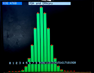
DISCLAIMER! The ROSC is not shown by the manufacturer or by me to have any reliable level of random generation. Further, of the three rp2040's I have tested, each gives a somewhat different oscillator speed, and different distributions of bits. Do not use this for any critical project without doing your own tests!
Filtering white noise using DMAcpu.(11jan2023)
The white noise generator was low-passed filtered using a 1-pole IIR, mostly just to see if the DMAcpu could do the arithmetic. It took a 38 step program about 4 uSec to compute a low-passed sample. I don't think this is a practical use for the DMAcpu, but it did test a lot of functions. The filter implemented is a simple one-pole IIR filter with a filter coefficient set by right shifting:
output = old_output + [(input - old_output) >> n]
It took a 38 DMA block program about 4 uSec to compute. Both channels are set to the DAC with the filtered output on channel A and unfiltered on channel B. Since my right-shift function only works with positive numbers, the actual function computed was:
output = old_output + (input>>n) - (old_output >> n)
Shown below are time domain and spectra waveforms for an n=4.
Top trace is the unfiltered noise in both the time domain, and the magenta spectra on the right.
Generating white noise from the DMAcpu. (7jan2023)
The program reads the ROSC random-bit
and shifts it into the sniffer data register. This shift register is then used as a seed for CRC32 hardware computation and the resulting scrambled bits are truncated to 12-bits for the SPI DAC to produce good sounding white noise. The machine runs at a sample rate of 50 KHz in the example code, but will run as fast at 500 KHz. The image below shows the spectrum at a sample rate fo 100 KHz. The spectrum is down about 6 db at 50 KHz, but flat through the audio spectrum. The time to generate a new audio sample is about 0.9 uSec. (the timing code in the linked program, but not shown below, adds 0.3 uSec.)
.jpg)
The code shows the simplifed block syntax.
Note that sniffer function alernates between add and CRC32.
Also, sending a value through the sniffer twice, in add mode, doubles it (shift-left)
// dma_sniffer_ set to add: add function code is 0xf in the calc field
build_block(&sniff_calc_mask, DMA_SNIFF_CTRL_SET, 1, STANDARD_CTRL);
// load a random bit fom ROSC to sniff data reg: dma_hw->sniff_data
build_block(rnd_reg, &dma_hw->sniff_data, 1, STANDARD_CTRL);
// pass shift-var thru the sniffer twice to the bit_bucket
build_block(&dma_noise_temp, &bit_bucket, 2, STANDARD_CTRL | SNIFF_EN) ;
// store back to shift-var
build_block( &dma_hw->sniff_data, &dma_noise_temp, 1, STANDARD_CTRL);
// dma_sniffer_ set to CRC32: CRC32 function code is 0x0 in the calc field
build_block(&sniff_calc_mask, DMA_SNIFF_CTRL_CLR, 1, STANDARD_CTRL);
// compute CRC32 build_block(&dma_noise_temp, &bit_bucket, 1, STANDARD_CTRL | SNIFF_EN) ;
// dma_sniffer_ set to add
build_block(&sniff_calc_mask, DMA_SNIFF_CTRL_SET, 1, STANDARD_CTRL);
// limit to 12 bit data: mask value is 0xffff000
build_block( &sniff_dac_data_mask, DMA_SNIFF_DATA_CLR, 1, STANDARD_CTRL);
// OR in the DAC control word
build_block( &dac_config_mask, DMA_SNIFF_DATA_SET, 1, STANDARD_CTRL);
// send to DAC
build_block(&dma_hw->sniff_data, &spi0_hw->dr, 1, (DMA_CHAIN_TO(fix_chan) | DMA_TREQ( DREQ_FORCE) | DMA_DATA_WIDTH(DMA_SIZE_16) | DMA_IRQ_QUIET | DMA_EN));
// unconditional jump to start of program
// push the DMA_blocks[0] address into the program counter (fetch channel read pointer)
// !!NOTE that this block throttles the machine to the frequency of Timer 3 !!
// To run at full DMA speed, change to DMA_TREQ(DREQ_FORCE)
build_block(&DMA_blocks_addr, &dma_hw->ch[fetch_chan].read_addr, 1, DMA_CHAIN_TO(fix_chan) | DMA_TREQ( DREQ_DMA_TIMER3) | DMA_DATA_WIDTH(DMA_SIZE_32) | DMA_IRQ_QUIET | DMA_EN) ;
Improved organization of the test program (3jan2023)
The
explicit DMA channel numbers were replaced with macros defining the actual channels so that the machine can be more easily used with other DMA-based protocols. The fetch/execute architecture is separated from the DMA program definition to make it easier to modify for new DMA progams. A macro is added to make the DMA channel control register specification more compact and easier to read.
More operations and better conditional jumps (2jan2023)
The program asks the user for two numerical values
then computes the sum, difference, shifted values and the sign of the first input value. Most of the explaination of this program is above, describing how each operation is decomposed into a series of data-moves.
An application: Direct Digital Synthesis (12/28/2022)
DDS is an attractive example because it requires fast, precise, timing, but is essentially a pointer increment followed by a table-lookup, then a 16-bit SPI load. In other words, mostly data motion. The DMA program takes to form of a linear set of instructions with no branching, just a loop back to the beginning of the program. Rather than running the DMAcpu at full speed, the loop back block is paced by one of the high precision DMA timers set to a fixed frequency. The program ran correctly up to the limit of the SPI DAC chip, 500,000 samples/sec, but for audio synthesis I used a lower frequency pace of 200,000 loops(samples)/sec. At that rate, the DMA machine ran about 25% of the time. The generated frequency matched the math to within the accuracy of my scope (about 0.1%).
Algorithm:
The DMA-machine program:
First DMA test program. (12/23/2022)
This program just toggles an i/o pin to trigger an oscilloscope, then runs through basic proof-of-concept
constructions. This program performs several operations using only DMA-logic. the DMA machine is completely asynchronous and independent of MAIN, once started. MAIN sets up the DMA machine program, defines variables for the machine, then prints the results of an ADD and OR operation on the serial console. No other microcontroller resources are needed (except memory, of course) to make the machine run. The execution speed is about 8 million blocks/sec. To make life easier I defined a macro to insert DMA control blocks into the array defining the program.
build_block(read_addr, write_addr, count, ctrl)
builds a DMA control block according to the specs in the data sheet.
Remember that control blocks are pulled one-at-a-time from the array, placed in the DMA1 hardware registers by DMA0, then triggered to perfrom the desired data move. After the move, DMA1 chains to DMA2 to reset the DMA0 write address to point to DMA1 control registers.
The DMA-machine program:
Not current below this line!
The DMA test program performs several operations using only DMA-logic. the DMA machine is completely asynchronous and independent of MAIN, once started. MAIN sets up the DMA machine program, defines tables for the machine, then prints the results of an ADD and NOR operation on the serial console. No other microcontroller resources are needed (except memory, of course) to make the machine run. The execution speed is about 200,000 blocks/sec.
The DMA weird-machine program:
Fetch/execute machine details:
The syntax given below assumes that DMA0 or DMA2 block images can be built by defining them using PLIB DMA commands, then copying the blocks (in the perparation stage) to the large array or arrays of block images. Macros hide the actual preparation and abstract the preparation to specifying the source address, destination address, source length (in bytes), destination length (in bytes), and the cell transfer length (in bytes). For example:
make_DMA2_block(LED_pattern2, (void*)&LATB, 64, 1, 64);
constructs and stores a block destined to be copied to the DMA2 control block which moves 64 bytes from a memory array, in a burst of 64, to the 1 byte
port B output latch. The effect is to generate a burst of output transitions on the port, when the block is later loaded into the DMA2 control register and executed.
Direct Digital Synthesis -- A possible practical use for the DMA machine (and optimizing execution)
DDS uses a table-lookup to send sine values to a SPI-attached DAC. It is possible to do DMA transfer to the SPI using framed mode, which autogenerates a chip select on the channel slave-select line. However, the chip select is limited to one pin and there can only be one peripherial on the channel. The serial DMA machine allows you to define an arbitrary chip select pin and manipulate it. The downside is that the maximum speed for the transfer is around 11.4 Ksamples/sec (when using the standard 192 byte full DMA block definition). The example code waits for a timer event, toggles the chip select, sends two bytes through SPI to the DAC, increments an array pointer, then auto-loops back to wait the beginning for a timer event. To turn off the machine, just freeze timer3 so that another SPI device can access the bus. The demo code does this with a serial command.
--
The rate-limiting step in the DMA weird machine execution is loading the 192 byte blocks for every operation. Careful consideration of the contents of the DMA control block suggests that the last two words are not needed for this machine (unless you try to use transport-triggered compare). This shaves 32 bytes off. Another 12 bytes can be pulled off the end because each control register has three shadow registers for transport-triggered logic operations. The first word of the block is constant and can be set once, saving 16 bytes. The net result is 132 byte transfers which speeds up execution by about 1.5 times. The sample rate jumps to 18 Ksamples/second. Code.
-- Just running the DAC transfer as fast as possible with NO time-trigger control speeds up the sample rate to 23 Ksamples/sec. The speed up happens because the block size is cut to 100 bytes (minimum). The minimum size does not include the ability to set up a time trigger using the DMA block interrupt detect hardware. Code.
-- Changing the code to use 2-byte transfers to the SPI channel requires a modified increment table which limits the maximum sine resolution to 128 samples/cycle. The scheme makes a table in which the increment is two, rather than one. The effect is to remove two blocks from the DMA-block DDS loop, and raising the maximum synthesis frequency to 23.6 KHz (still with timer control). For the DDS sinewave this gives a frequency range from 2.95 Hz for a 8-sample sine to 184 Hz for a 128-sample sine. The 23.6 KHz synthesis rate corresponds to a timer interval of 1700 cycles. This means that changing the sample rate allows frequency control of better than 0.1%. Changing the length of the sine table by one sample yields frequency control of 1/(sine_table_size).
Code. <<use this version for DDS>>
Pseudorandom or random sequence generation
This example uses the CRC hardware module to generate a pseudorandom 16-bit
number sequence. OPtionally, reading a floating ADC input adds some entropy to make the sequence truly random, but not cryptograhic quality. The sequence is output through the SPI DAC interface for spectral analysis. If the ADC is used, it is read every eighth interation of the LFSR, with 8-bits of the ADC reading XORed with the lower 8-bits of the LFSR seed. Running the CRC LFSR, emitting the SPI data, computing the conditional ADC read all runs at about 10KHz. The code needs a 16-bit SFR to use as a 16-bit ALU. The OCR5 set/reset registers were used. This version of the code optimizes for speed by eliminating possible timer control, so the system just runs as fast as it can. Eliminating SPI output would speed up random number genration about 30%. Eliminating the ADC read would speed it up by about 25%, but makes the sequence completely repeatable, and dependent on the initial seed chosen. The output noise spectrum drops with a 3db point at about 25% of the sample frequency and a minimum at the sample frequency at least 30db down.
Code (with ADC read every three LFSR operations)
Spectrum of DAC output with no ADC reads. Sample rate is about 16.8 KHz.

Older versions:
Time synced operation:
It is possible to sync overall machine operation to a timer by modifying one DMA2 block definition to trigger a transfer on a timer event. Note that this is a blocking-wait, which kills DMA execution until the timer event. The could be useful for a small program that, for example, sends a word to the SPI channel on a regular schedule to run a DAC. The sequential machine would wait for a timer event, drop the chip-select line, transfer a word to the SPI buffer, raise the chip-select line, then loop to wait for the next timer event. The DMA2 block definition which waits, then executes a NOP could be:
DmaChnOpen(2, 0, DMA_OPEN_AUTO);
DmaChnSetTxfer(2, &inc_value, &bit_bucket, 1, 1, 1);
DmaChnSetEventControl(2, DMA_EV_START_IRQ(_TIMER_3_IRQ));
DmaChnSetEvEnableFlags(2, DMA_EV_CELL_DONE);
DmaChnEnable(2);
memcpy(DMA_blocks+length_of_block*N, &DCH2CON, length_of_block);
N++;
This
code runs the main DMA loop at 100 Hz by waiting for timer3 event.
Optimizing test code execution speed
-- The execution speed of the DMA machine is limited by the need to load a 192 byte control block for each operation. By reducing the felxibility of the machine, certain chunks of the DMA2 block do not need to be reloaded each time. An optimized version with about 1.4 speed-up minimizes DMA2 block updates, but still allows full functions described above. optimized code.
The minimum execution time for one block dropped from 10 µsec to 7 µsec because the bytes per block were reduced from 192 to 132.
--
It is possible to optimize further, but the ability to trigger a block from an outside source (perhaps a timer) is lost. By eliminating the copy of the interrupt control registers, the copy count drops to 100 bytes, and the minimum block execution time drops to 5.5 µsec. The general test code above still runs, but time sync is much harder. The DCHxSSA, source address, register is the first address copied and the DCHxCSIZ, cell size register, is the last (see datasheet page 52).
A different (and probably inferior) way to run the Fetch/Execute cycle
The method used above is optimal in terms of wasting no cycles because the fetch/execute cycle is asychronous. As soon as an operation finishes, then next one can start. However, all four DMA channels are needed to make the machine run. One channel is the fetch unit, another is the execute unit, and two others are just used to clear interrupt flags in the first two channels.
If a timer and output compare unit are used to generate two time-synched interrupt flags, then the two (fetch and execute) DMA channels can be triggered by the interrupt flags. The up side of this scheme is that it frees up two DMA channels. The down side is that the slowest operation determines the execution rate of the machine. Most operations are fairly fast, but add is much slower and branch is a little slower. Including add operation drops performance by a factor of 10. Branch operation drops performance by a factor of 2.5. Tuning becomes quite dificult. But for reference, a running code (without add operation) is included which runs about 0.4 as fast as the async code. Code.
Copyright Cornell University April 10, 2024