James Du (jsd46)
Peter Greczner (pag42)
We used a Sony Handicam to capture and send video to SDRAM and an RS-232 serial port to send images to SRAM. The stored images are combined accordingly and sent to a VGA display.
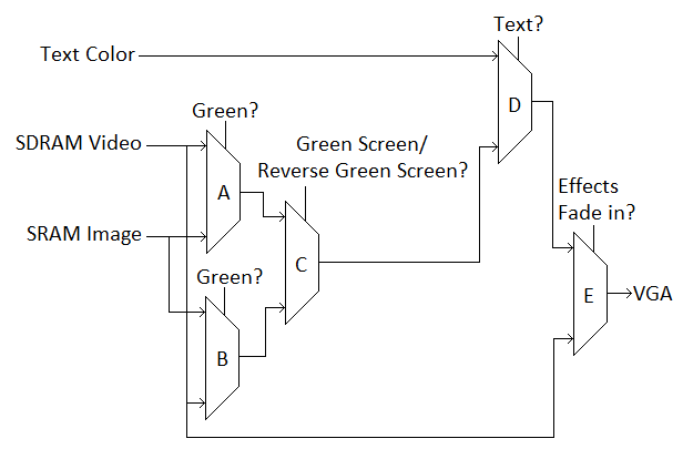 Figure 3 shows how signals propagate from the camera and RS-232 serial port to the VGA display. Each line carries the value of a pixel and the modules know the current horizontal and vertical position of that pixel. Mux-A is used for the green screen effect. If the pixel from the SDRAM video feed is considered green, mux-A outputs the pixel from the SRAM image instead of the SDRAM video feed. Mux-B is used for the reverse green screen effect. If the pixel from the SRAM image is green, mux-B outputs the pixel from the SDRAM video feed instead of the SRAM image. Mux-C is used to choose whether to output the green screen or reverse green screen. Mux-D is used for writing text to the screen. If the current pixel's position is within the bitmap of a letter that's supposed to be written to the screen, mux-D outputs the color of text displayed on the screen instead of the output from the green screen/reverse green screen effects. Finally, mux-E is used to fade in the effect. If the effects are supposed to be faded in, mux-E outputs the combination of all the other effects. If the effects are not supposed to be faded in, mux-E outputs the SDRAM video feed with no effects added in. Video CameraThe video camera interfacing was handled by the DE2_TV provided by Terasic Technologies in a CD that came with the DE2 board. The video camera RCA video output is connected to the DE2 board. The signal is in ITU656 format. The signal gets converted to YUV 4:2:2 format, down-sampled from 720 to 420 horizontal pixels, and then stored in SDRAM. When the image is read out from SDRAM, the pixels get converted from YUV 4:2:2 to YUV 4:4:4, and then to RGB format. In the DE2_TV module, the RGB signal is sent to the VGA output. We intercept this signal and add effects before feeding it to the VGA output.Serial Image TransferThere were two possible ways for us to implement the RS-232 communication. We could choose to instantiate a NIOS II microprocessor and have it include a UART module or we could create our own hardware receiver and transmitter UART modules from scratch. While it would have been easier to go the NIOS II route the problem was that the NIOS II microprocessor needs the SDRAM as its memory, and we were currently using that memory for holding the video image data. In order to avoid any conflicts we decided it would be best to develop our own hardware receiver and transmitter.RS-232 Protocol DescriptionIn order to develop these modules one has to understand how RS-232 protocol works. There are a lot of different options that one can choose, but we decided on the following, fairly standard, options for communication – 8 data bits, 1 stop bit, 1 start bit, no flow control, no parity bit. The baudrate that we used changed throughout development, but initially we started with a fairly slow and safe baudrate of 9600 baud. The end product runs at a baudrate of 115200 baud.To receive a byte of data you have to first listen for the start bit. The start bit is a logical zero on the UART receiver and you recognize it as the start bit because when the UART receiver is idle it has a logical one outputted. Once the start bit is received the following eight clock ticks will posses the data portion with the least significant bit being passed in first. After all 8 data bits are received you listen for a stop bit which will be a logical one. If a logical one is not received then you know that an error has occurred and you have probably lost sync or connection with what you are receiving from. The image below illustrates the protocol. 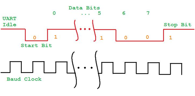 There is one intricacy in designing a receiver that isn’t initially noticeable by simply following the protocol. We initially ran into problems that we were getting more bit errors that we typically should have gotten. This was thought to be a problem that we could not generate a baud rate exactly equal to 9600 baud. Since our baud rate was slightly off this meant that every now and then the receiving clock would lose sync with the transmitting clock (which is why error detection was implemented to correct this) however we were receiving possibly too many errors. After reading a bunch of literature on RS-232 error detection we found out that most modules sample the idle line at 16 * BaudRate. An example we found showed how to do it at 8 * BaudRate and suggested that this should be fairly sufficient and we implemented the examples suggestion. This greatly reduced the amount of bit errors received. The reason for this is that when you sample at 8 times the baudrate you ensure that you do not miss a potential start bit due to clock error. Then once your 8 times fast baud clock finds the start bit it resets the normal baud clock. Then you are almost guaranteed no error in the normal baud clock since it is always starting in sync with the transmitted data. To transmit a byte of data this same protocol is followed. The transmitter constantly outputs a logical one, and then when it wants to begin transmitting it changes to logical zero, followed by the 8 data bits, and then back to logical one for the stop bit. It is up to the receiver to make sure that data is received correctly provided that the transmitter follows protocol. You do not need a fast baud clock for transmitting since it is the receivers job for staying in sync. Receiver and Transmitter Module DesignBoth the transmitter and receiver were designed to follow the protocol above. The receiver works by sampling the idle line at 8 times the baud rate and once a start bit is detected it enters a state machine that collects the data. Once the 8 data bits are collected it listens for the stop bit. If a stop bit is not detected it enters its error correcting mode. In error correcting it checks for one of two things to occur. The first is that it receives 10 logical ones in a row which would signal all idle bits. The second is that it finds a bit spacing equivalent to a start bit followed by 8 bits followed by a stop bit which would signal data and it knows its back in sync. Any data received during error correcting is lost, but the main point is that the receiver is now back in sync with the transmitter.The transmitter works by following the aforementioned protocol and writing back whatever data is issued to it at the time of a transmit request. Packaging the DataTo send the image data it became apparent to us that we needed a way to ensure that what was being transmitted was what was actually received. Initially we had just assumed/hoped that the serial communication would be accurate enough that we could just send the data and let a FPGA state machine choose where to output the data. However, when data was lost this caused the image to skew itself and some pixel colors would be wrong. In an effort to fix this problem we needed to implement some form of bitwise error detection. Research showed that generally a CRC is done on packets of data or you could do a parity check. We felt that a one bit parity check would probably not be enough to ensure accuracy of the data so the packaging and CRC route was chosen.When data comes into the receiver it is outputted to a PacketManager module. This module packages the incoming bytes into a packet of length 16 bytes. The format of the packet is 15 bytes of data followed by 1 byte of CRC. Now, we didn’t implement an actual CRC check, but rather a very quick yet suitable XOR. All 15 bytes of data were XOR’ed and this result was the 16 byte in the package. Once a packet is assembled the data bits are sent to our CRC module which performs the XOR. The result of this XOR is then compared to the 16th byte of our packet. If the CRC matches the 16th byte the transmitter is told to send a byte valued at 255 indicating a success, but if it does not match it sends a byte valued of 0. Then retransmission can take place if needed. Dealing with loss of synchronization – TimeoutsA previous problem which was mentioned was a loss of synchronization with the transmitting and receiving module. It could happen that the receiving module enters a state that it can’t get out of because the transmitter keeps sending data and the receiver can never fix its error. If this happens then the transmitter will never have a finished packet and thus cannot send back either an ACK or NACK of successful receipt. Because of this potential problem we implemented a method to detect timeouts.Whenever a new packet is started it is given a start time based on the FPGA run time. This start time is 128 bits long and should never overflow during the course of execution as it increments on the 50MHz clock (unless you run your FPGA for about 2^23 years). Then each clock cycle the packet manager checks to see if the time between the receipt of the first byte in the packet and the current byte is greater than 0.2 seconds. If it is greater than we believe that some error has occurred and we need to issue a timeout error. The packet manager then resets the receiver and tells the transmitter to issue a timeout NACK to the host receiver. This NACK is byte valued at 128 to indicate a timeout has occurred. Baudrate GenerationTo generate the baud rate we used the 50 MHz clock and found an appropriate integer divider and incremented an accumulator. One the accumulator was equal to the divider we new that a baud clock tick was appropriate. The error rate depending on the desired baud rate was generally less than .001%.Writing the Image to SRAMOnce a packet is fully received and checked that it contains no errors we “unpack” the data and write it appropriately to SRAM. There are five methods that we created for unpacking the data and writing to SRAM – each is used for a different application of displaying the image.Displaying 640x480 images:The first three bytes in this type of image contain a start X and Y coordinate. The reason that three bytes are needed is that 640 maximum value requires 10 bits and 480 maximum value requires 9 bits for a total of 19 bits which can only be held in 3 bytes or 24 bits. The following 12 bytes of the packet hold color values for the 12 pixels that immediately follow the start X and Y coordinate inclusive of start X and Y. The drawing state machine then cycles through these 12 bytes of data and increments the draw X by one for each subsequent data byte. If it gets to a point where X > 640 it just does not draw it to avoid drawing out of bounds. On each cycle the SRAM address and data registers are set to indicate the pixel position via the address register and color value via the data register.Displaying 320x240 images stretched to 640x480: Again the first three bytes specify the start X and start Y values. Again, the next 12 bytes represent color data. This time the data register duplicates the color data in order to stretch out the image in the X direction. The reason why this stretches it is because we store the image as 320 16-bit color values for each row. So essentially, each data block holds two pixel values that are adjacent to each other. When we duplicate the 8 high bits and low bits of the data this stretches the image. To stretch in the Y direction we write to SRAM by shifting the start Y value by 1 (doubling it) and adding either 0 or 1 depending on if it is the first row or second row to be saved to SRAM. Displaying 320x240 images stretched to 640x240: This works the same exact way as stretching to 640x480 except that we do not stretch in the Y direction. This means that the start Y value is not shifted right by 1 and instead is used directly in the SRAM destination address. Displaying 320x240 black and white images stretched to 640x480: In this mode we stretch a 320x240 black and white (binary) image to 640x480. To do this we again specify the first 3 bytes as start X and start Y values. Then, the next 12 bytes of 96 bits represent 96 pixels. The state machine loops through each of these 96 pixels and stores to SRAM either the color white or black depending on the pixel value. It stretches in the X and Y direction the same way as in the other stretch routine. Because we can write 96 pixels at once this method of image transfer is very quick. Direct Draw Method: One other method that was implemented was that in each packet we specified 3 direct locations and color values to be drawn to. In this method the packet was set up as 3 bytes for image location followed by 1 byte for image color data. Since this took four bytes we could hold 3 of these pixels in a packet and 2 bytes were wasted. This method is very slow compared to the other methods but has the advantage of being able to draw directly to any pixel value instead of sequentially. You could imaging this method being used to draw a title overlay instead of an actual image. This method only worked for 320x240 image resolutions. VGA InterfaceGetting 640x480 resolution out of SRAMSRAM is not big enough to store 640x480 16-bit pixel information. However, it can accommodate 320x480 16-bit pixel information. Therefore to get a resolution of 640x480 we need to limit the amount of color information for each pixel. The logical approach is to have each pixel have a color depth of only 8 bits instead of 16 bits. We divided up the RGB values into 3-bits for red and green and 2-bits for blue. When it came time to read from SRAM and display on the VGA these 16 bits were read and if the least significant bit of the X part of the SRAM address was a 0 then we would output the left pixel or data bits 7:0 and if it was a 1 then the right pixel or data bits 15:8. The red, green, and blue components are required to be 10 bits according to the VGA parameters. To get 10 bits for each we used the following code:
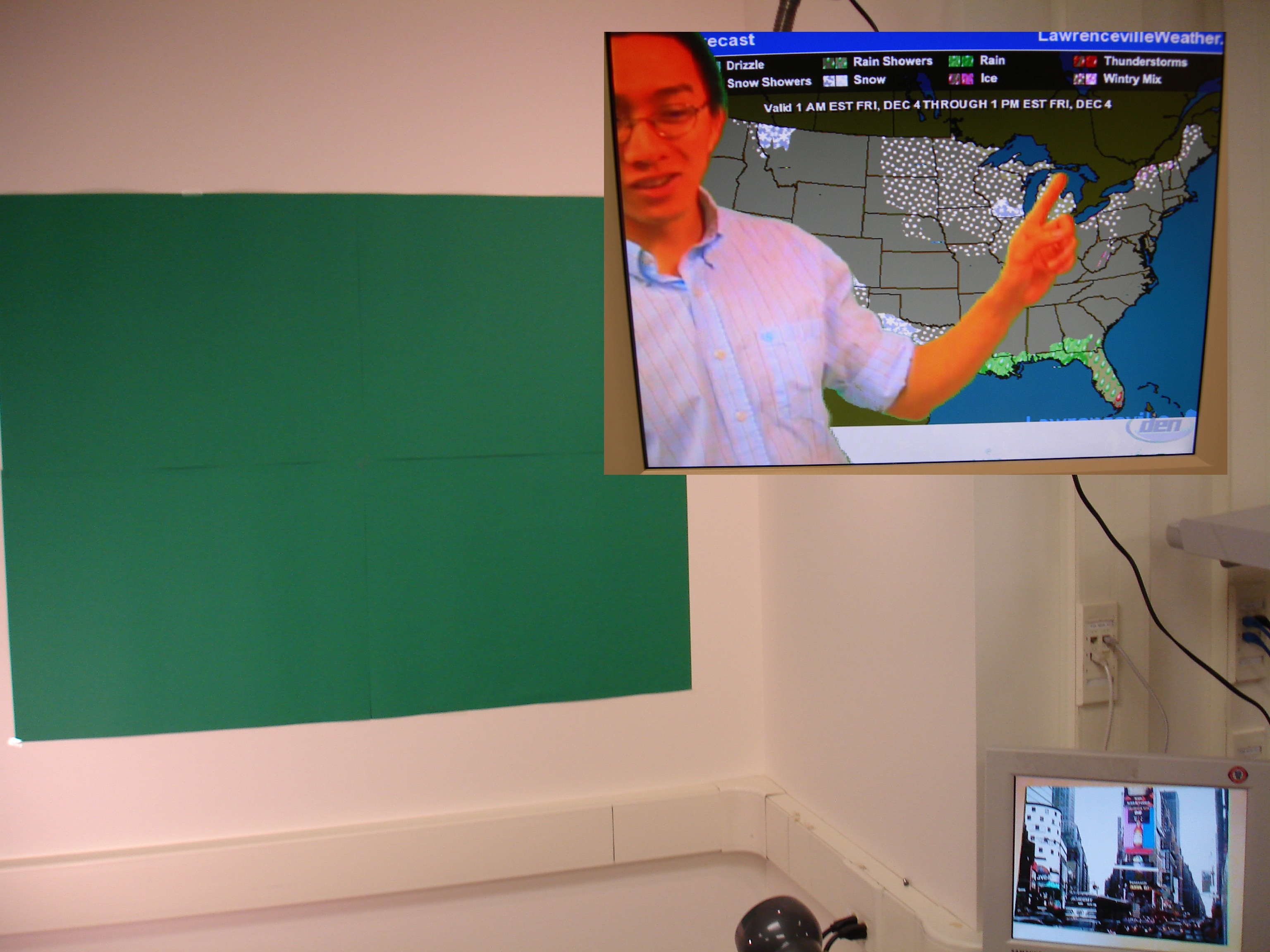
Green Detection in Video for Green ScreenThe VGA output receives one pixel at a time. Each pixel goes through green detection. A pixel is determined to be green if its green is above a certain threshold, its red is below a certain threshold, and its blue is below a certain threshold. There is a tradeoff between having green artifacts at the borders of green areas and detecting green in areas that are not part of the green screen.If the green threshold is set too high, and red and blue thresholds are set too low, the green screen might not be green enough to be classified as green, and any reflections or slight deviations from green on the green screen will not be classified as green. Green threshold being too low also results in large green borders between the green screen and anything that appears in front of it. If the green threshold is set too low, and the red and blue thresholds are set too high, areas that are not part of the green screen will be classified as green. During testing, areas that were green were set as white; setting the green threshold too low made objects appear as if electricity were surging through them. To match the thresholds to the green screen, we set the thresholds with switches. We tuned the thresholds until the green screen was considered green and there was no green in all of the other objects in the video. Green Detection in an Image for Reverse Green ScreenSince we know the exact green value that we are drawing into the image that we are using for reverse green screen, we can look for an exact green value rather than setting thresholds. Other than image and video quality, reverse green screen works perfectly with no artifacts for all of the images that we tested since we do not have to worry about false green detections. If any part of an image happens to be the exact value that is considered green, we could tweak one of its bits, which would be unnoticeable except to the green detection.Fading Effects In and OutThis effect doesn't make sense for green screen, but it is useful for reverse green screen effects and text. A 25 bit counter is used for this effect. When a button is pressed, the counter, which runs off of the 27 MHz clock, starts counting until it maxes out. If the counter starts at 0 it counts up; if the counter starts at its maximum, it counts down. The top 10 bits of the counter are bitwise &'d with the effects output. The complement of the top 10 bits of the counter are bitwise &'d with the regular video input. The counter length was chosen so that it would take 1.24 seconds to fade in and out so that the duration is long enough for a human viewer to notice. This scheme allows the regular video feed to fade out and video feed with effects to fade in at the same time, and vice versa.Writing Text to the ScreenA keyboard is connected to the PS/2 port of the DE2 board. When keys are pressed, they are displayed at the center of the screen if effects are faded in. A 16 keystroke buffer is used to store the message displayed. When the first key is struck, it is displayed at the left most position of the 16 keystroke buffer. When the next key is struck, it is displayed 8 pixels to the right of the first keystroke; and so forth. When the end of the buffer is reached, the keystrokes wrap around and start writing over the first keys struck. The keyboard interface was obtained from http://www.johnloomis.org/digitallab/ps2lab1/ps2lab1.html. These modules read in the serial stream sent from the keyboard to the PS/2 port. A simple state machine is used to determine which keys are struck: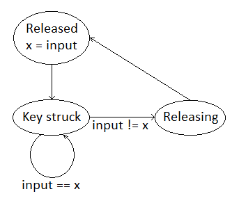 There are two states for releasing a key because two bytes are sent when a key is released. When a key is initially pressed, the byte that corresponds to it is sent. If a key is pressed and held, the byte that corresponds to the key is sent over and over again. The mapping between the byte sent from the keyboard and the character the byte represents was obtained from http://www.sm.luth.se/csee/courses/smd/098/lab31.pdf. Each time a key is struck, a number that corresponds to its character is stored in the sentence buffer, and a pointer to the current register being written to in the sentence buffer gets incremented. The pointer returns to the beginning of the buffer after the pointer gets to the end of the buffer. Numbers 1 through 26 corresponds to letters A through Z. The bitmaps for the characters were obtained from http://users.ece.gatech.edu/~hamblen/book/instruct_se.htm. The Mega Function Generator was used to store and access the .mif file. 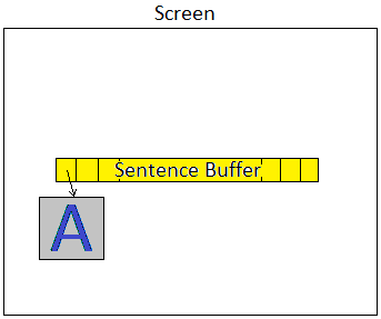 The image of text on the screen is not stored in RAM. Writing text to the screen is implemented using each pixel's coordinates. A module called screenWriter determines whether or not to color in a pixel because the pixel is part of a letter. If a pixel's coordinates are in the white area in Figure 3, screenWriter tells higher level modules to output regular video for that coordinate because the pixel definitely cannot be part of the text. If a pixel's coordinates are in the yellow "Sentence Buffer" area, screenWriter looks up the bitmap that represents the character in that area. If a pixel's coordinates are in the grey area of the bitmap, then screenWriter once again tells higher level modules to output regular video for that coordinate. If a pixel's coordinates are in the blue area, then screenWriter tells higher level modules to output text color for that pixel. |