Hardware Design
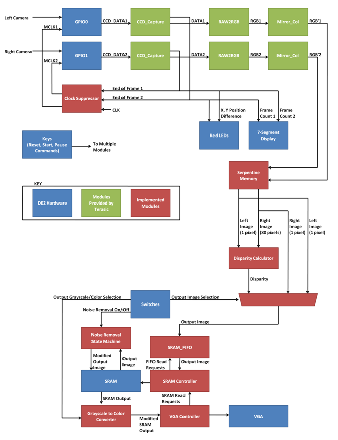
The structure of the entire system is summarized in the figure above. We have the inputs from the two cameras arriving through the GPIO ports. The inputs are fed through three decoding modules provided by Terasic: CCD_Capture, RAW2RGB, and Mirror_Col. Status signals from CCD_Capture are outputted to LEDs and 7-segment displays to aid debugging. Furthermore, the end of frame status is used by a clock suppressor that stops the clock input to either camera when it starts leading the other camera, thereby maintaining synchronicity between the two camera outputs. The processed image from the cameras are converted from RGB values to 8-bit grayscale intensities and fed to the serpentine memory, which stores the past 80 pixel values of the right camera and the past 1 pixel value of the left camera for disparity calculation. Three potential output signals are then generated – the original grayscale image captured by the left camera, the original grayscale image captured by the right camera, and the disparity map calculated from the images from the two cameras. One of these image streams is fed to a SRAM FIFO (first-in, first-out) module, which acts as a temporary buffer storage for the SRAM. When the SRAM is not busy outputting to the VGA, data is read off of the SRAM FIFO and stored in the SRAM. The SRAM Controller handles this operation. Furthermore, the data read from the SRAM for output to the VGA is passed through a grayscale to color converter filter, which converts the 8-bit grayscale value to a color hue when the feature is enabled through a dipswitch. Finally, a noise removal state machine can process the entire screen image stored in SRAM and reduce noise. While the noise removal state machine is accessing the SRAM, the SRAM controller does not save any incoming data to the SRAM, though the VGA continues to access the SRAM.
Serpentine Memory
The serpentine memory module, as referred by our primary source by Georgulas et al, is essentially another term for temporary pixel data storage. This memory is used to help us store the relevant previous rows of pixels which can be used to process within a window or range of disparity values. To better explain how the Serpentine memory works, consider an mxm window in which to compute the local variation. Pixels are read from left to right, top to bottom, starting with the top left corner traversing through the first row. The serpentine memory stores the pixel data of the first m rows and the mth column of the mth row. From then on, the window furthest to the latest has all available pixels to process, and a local variation is computed. At the next clock cyle, the window moves one pixel to the right. Since the window consists of one new pixel, that pixel can be read in and processed within one pixel clock cycle.
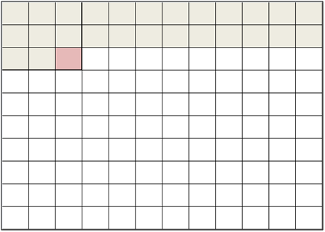
Figure 1: First local variation is computed when all previous pixels are read and stored.
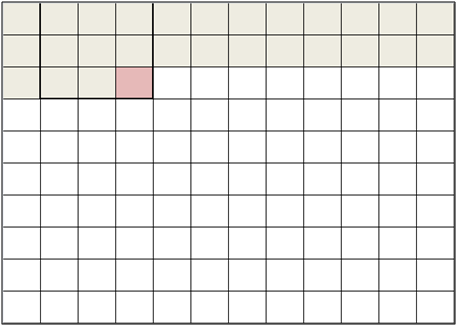
Figure 2: A new pixel is read out, and the window is shifted to the right.
This process occurs until the end of the row. The module then waits for the first m pixels to be read out in the next row, and the local variation is computed thereon. The pixels of the next row overwrite the data from the first row of the serpentine memory. This allows the temporary storage array to be consistently the same size at each pixel time step while allowing enough pixel data to be stored in order to process the pixels within the windows. At the end of the frame, the Serpentine memory is reset.
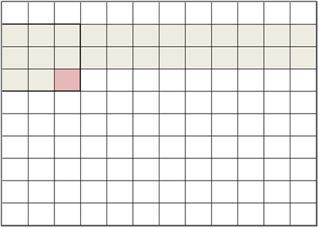
Figure 3: The first two pixels are read out until the local variation can be computed again for the next row. We then go back to Figures 1 and 2.
When our program was simplified to using 1x1 windows, the Serpentine memory is dramatically simplified to having one row of temporary storage across a scan line in order to store the pixel data used for disparity calculations. There is also no longer any need for Serpentine memory for pixels in the left image.
Local Variation and Window Selection
We implemented a module that computes the local variation within a window of a specified size using the following formula:
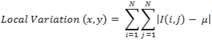
where I(i,j) is the pixel intensity at coordinate (i, j) and μ is the average grayscale intensity of the image window. This value is a good indication of how flat a particular area of the image is. If an area is fairly flat, like the window showing a section of a wall that’s parallel to the image plane, a large window can be used when computing the disparity. Reversely, if the local variation is very large, a small window size should be used so that the differences in depth can be detected. The output of the local variation module is then fed into the window selection module, which involves a simple thresholding procedure to determine which window size to select. Because we had to condense our computation down to one size, these two modules were later removed from our program.
Disparity Calculation
This module takes the image pixel data from the serpentine memory for the left and right cameras and computes the sum of absolute difference for each disparity value. The formula is shown below:
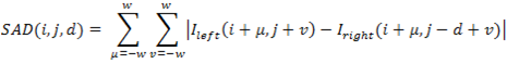
where I_left and I_right represent the pixel grayscale intensity for the left and right image respectively, d is the disparity value, and w is the window size. Since we are using a 1x1 window, the SAD is simplified to:
![]()
for 0 ≤ d ≤ 80
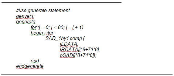
The SADs are implemented through a Verilog generate statement, with each output independent of the other. An example of the Verilog code is shown below:
We then find the minimum of all 80 SADs using a binary tree algorithm in order to parallelize the comparator logic by using the least number of computational cycles. In a linear search, it would take n cycles to find the minimum of n numbers. With a binary search, 40 comparisons can occur in the first cycle, 20 comparisons on the second cycle, and so forth. This results in a maximum of 6 cycles, which greatly enhances the logic throughput. The output of this module is the disparity value corresponding with the minimum SAD value. Since the disparity only reaches a maximum of 80 pixels, the output is sampled nonlinearly across the intensity spectrum from 0 to 255. We would like have close to a linearly gradual decay in disparity as an object is positioned further away from the camera. This means that disparities at close range change relatively slowly while disparities at long range change relatively quickly. We devised the following formula to determine the output depth values:
![]()
Clock Suppressor
The clock suppressor feeds clock signals to each of the two cameras. The goal of the clock suppressor is to synchronize the operation of the two cameras so that one camera does not lead the other. If the cameras are kept synchronous, we will be able to perform disparity calculation in real time because we will be able to compare pixels at the same positions in the two cameras. If one camera is leading, the clock suppressor stops the clock feeding into that camera until the other camera catches up. This is performed at the end of the frame, when the positive edge of the frame valid signal indicates that a camera is about to start processing a new frame. If one camera exhibits a rising frame valid signal before the other, its clock is halted.
To a degree, we treat the modules provided by Terasic as black boxes. Since none of the reset modules were able to slow or stop the operation of one camera until the other caught up, we ended up implementing this clock suppressor to stop the operation of the camera at the root, by starving the camera of a clock input.
SRAM FIFO
The SRAM FIFO is a simple 16-bit 256-depth FIFO (first-in, first-out) buffer that is generated by Quartus II’s MegaWizard. The role of the FIFO is to provide a buffer to the stream of data that must be saved to the SRAM. This buffer is needed because although there is a constant stream of data that must be saved to the SRAM (due to the constant stream of data outputted by the cameras), the SRAM must occasionally spend time outputting data to the VGA. The buffer prevents data from being discarded when attempting to write to the SRAM when it is busy outputting to the VGA.
Grayscale to Color Converter
The disparity value and the direct output images from the cameras are saved as 8-bit grayscale values to the SRAM. To improve the contrast between two similar grayscale values, the grayscale spectrum can optionally be converted to the hue spectrum. For colors with maximum saturation and half maximum luminosity, the hue spectrum progresses as follows:
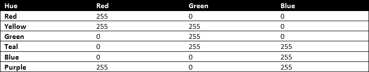
Reserving the first 16 grayscale values to represent black, we form the following mapping between grayscale values and hues:
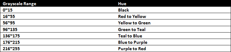
This module combinotorially maps the input grayscale range to the hue spectrum, outputting Red, Green, and Blue values of the hue corresponding to the input grayscale value.
SRAM Controller
The job of the SRAM Controller is to efficiently handle the regular read requests from the VGA controller and store the stream of inputs buffered by the SRAM FIFO so that the FIFO does not overflow. Several techniques are utilized to improve the performance of our SRAM controller.
First, since our pixel data is only 8 bits, we only need to read once for every consecutive two pixels to display on the VGA screen. This means that SRAM is accessed for the VGA only when the lowest bit of the currently displayed X coordinate is 0, in addition to the usual condition of horizontal sync and vertical sync both being high. This effectively reduces the time that the SRAM is occupied by the VGA by half. There are some challenges implementing this method, such as the fact that the output of the SRAM must be stored to a buffer register for the VGA to read instead of the SRAM when the VGA gets to displaying the next pixel.
Second, since our pixel data is only 8 bits, we only need to write once for every two new pixels streamed from the cameras. This is more of an optimization that is performed before the SRAM FIFO stage – two pixel’s worth of data is packed in a single FIFO block instead of just one. Again, this is performed by having a buffer register that temporarily stores the value of one pixel until the value of the second pixel comes in.
We also need to be careful when reading from the FIFO. We need one cycle after requesting a block of data from the FIFO before we can read that data. Then, on the next cycle, the block of data must be written to the SRAM. If a SRAM read request from the VGA interrupts this sequence, we must be careful to turn off the read request from the FIFO, but to eventually read the output port of the FIFO and write it to SRAM when the VGA controller is done reading from the SRAM. We use a 1-bit flag register to properly process this case.
Noise Removal State Machine
The Noise Removal State Machine is actually just another mode at which the SRAM Controller operates. Once noise removal mode is enabled, when the SRAM Controller finishes copying an entire frame from the input stream from the cameras, it enters noise removal mode. In this mode, the SRAM Controller traverses through the entire image frame stored in SRAM, performing the following algorithm on each pixel:
1. For each of the eight surrounding pixels, if a low-depth (black) pixel is detected, add 1 to a counter.
2. If the counter is greater than 6, set the center pixel to black.
This effectively removes much of the background noise, which consists of many solitary pixels of random grayscale intensities in a sea of black pixels.
Since two pixels are stored per SRAM address, this algorithm requires only six SRAM reads and two SRAM writes to process two pixels. Furthermore, the SRAM_FIFO is not used for writing to the SRAM because the SRAM writes are not constrained to a particular window of time as is the case when processing an input stream. The six SRAM reads are shown below:
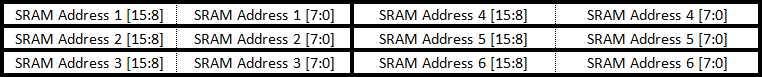
This corresponds to a 4x3 block of pixels outputted to the screen, with the top 8 bits of each address representing one pixel and the bottom 8 bits another. From these pixels, we can perform the aforementioned algorithm on two pixels – the pixel stored at the bottom of address 2 and the pixel stored at the top of address 5. Each of these two pixels has all eight surrounding pixels known.
A simple state machine is used in this mode to perform the sequential processing. The state transition diagram for the state machine is shown below:
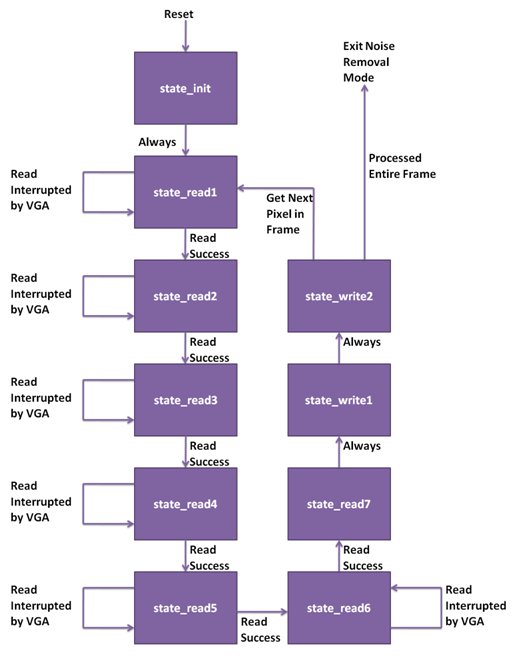
The state transition diagram is rather simple. state_init initializes the registers used in the state machine and provides an entry point to the state machine. state_read1 through state_read7 are used to read the six SRAM addresses. There is a one cycle delay between when the read address is specified and when the output from the SRAM can be stored. Thus, a read address is specified in state_read1 through state_read6 and the output from the SRAM is stored in state_read2 through state_read7. Each of these states except for state_read7 has a detection mechanism that detects if a read operation was interrupted by the VGA reading from the SRAM. If the read operation is interrupted, the state machine stays in the same state and attempts the read operation again. Once the read operations are complete, up to two writes occur in state_write1 and state_write2. Since writes to the SRAM are complete on the cycle that the write parameters are specified, it is impossible for the writes to be interrupted by the VGA. Once an entire cycle of reads and writes is complete, the routine is repeated for the next pair of pixels in the frame. Once the entire frame is processed, noise removal mode is exited and the system starts to read the stream inputs from the cameras once again.
VGA Controller
We reused the VGA controller we have been using throughout the semester. Special thanks to classmate Skyler Schneider for providing the VGA controller.