"An FPGA based real-time morphological image processor to show Edge-detection, Grayscale, Dilation, Erosion, Opening and Closing."
Project Soundbite
Introduction top
Mathematical morphology is a theory and technique for the analysis and processing of geometrical structures, based on set theory, lattice theory, topology, and random functions. It is most commonly applied to digital images, but it can be employed as well on graphs, surface meshes,solids, and many other spatial structures. Often times, people would apply dilation, erosion, opening, closing and edge detection when they determine to use mathematical morphology to address pictures.
Our project is a FPGA based real-time Morphological Image Processor. Projects that deals with image processing usually can't address real time image calculation. But with FPGA we may make this happen due to its fast calculation. We use M4K blocks instead of normal registers to store pixels which might exceeds the total number of registers on board, we also utilize shift registers to address data in pipeline so that we can fasten the speed when it's processing.
We aims to realize dilation, erosion, opening, closing and edge detection using Cyclone DE-2 and Terasic TRDB-DC2. Video signal is sent to the board’s decoder chip from a camcorder via a composite cable. Once decoded to RGB, the signal will pass through edge detection, binaryzation that we created in hardware. Then the pixel data will be sent to the board’s VGA driver and outputted to a monitor. The user is able to select both binary threshold, exposure threshold and also the sobel threshold by using the DE2’s switches. There are also options to display in grayscale image, binary image and sobel schemes selectable by the switches as well.
Principle top
Mathematical Morphology (MM) is a theory and technique that is widely used in analysis and processing of image, especially geometrical structures. It is based on the Set Theory, Lattice Theory, Topology and Random Functions. MM is usually used in processing of digital image, but it can also be employed in many other spatial structures. MM consists of a set of operators that transform images according to some certain characterizations, including shape, convexity, connectivity and geodesic distance, etc. Usually MM is conducted in binary images, but it can also be extended to grayscale functions and images.
The basic operators of Mathematical Morphology include: Edge Detection, Binary Dilation and Erosion, Binary Opening and Closing, Skeleton Extraction, Ultimate Erosion, Top-hat Transform, Morphological Gradient, Watershed, etc.
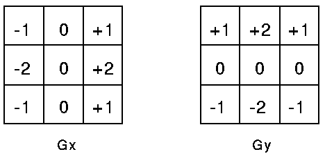
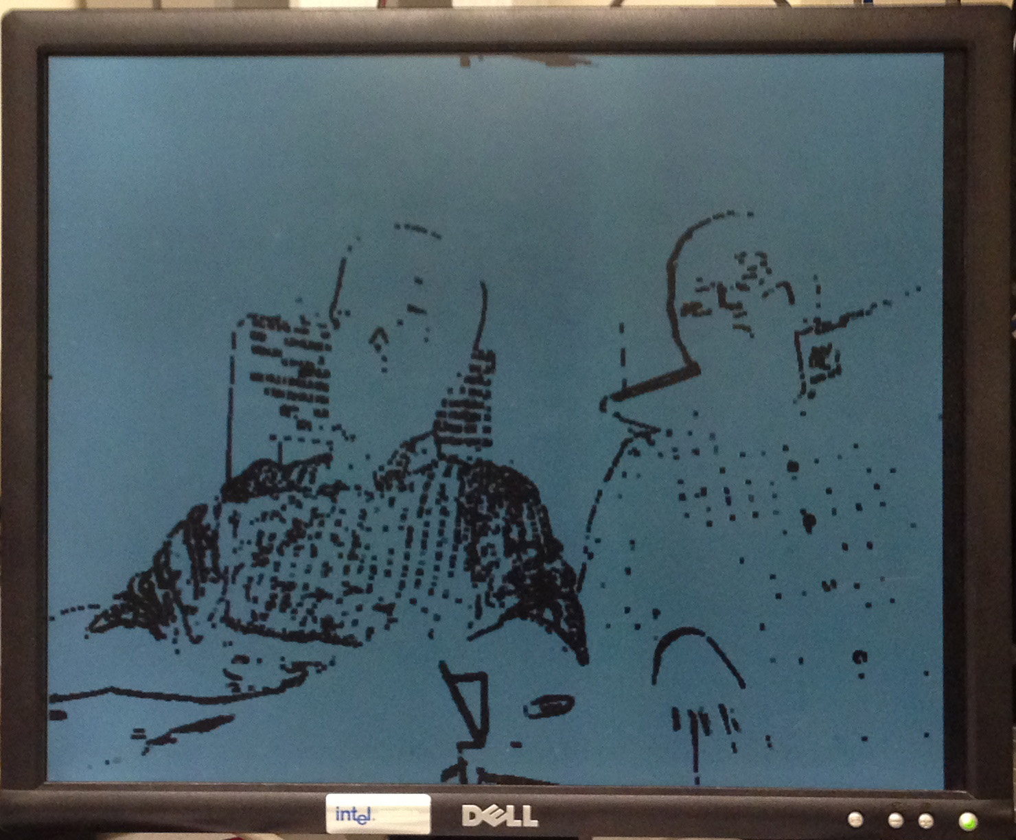
Edge Detection
The Sobel operator is used to perform a 2-D spatial gradient measurement on an image so that to emphasize the regions of high-spatial frequency, which correspond to edges. Technically, it is a discrete differentiation operator, computing an approximation of the gradient of the image intensity function. Employing this Sobel operator at any pixel of an image will produce corresponding grayscale vector and its normal vector.
The operator consists of a pair of 3x3 convolution kernels as shown in figure below. The two filters compute both the vertical edges (the left one) and horizontal edges (the right one). The filters are convolved with the entire input image. The middle pixels are weighted more heavily than the outer pixels, since they are closer to the pixel in center of grid and thus have a higher impact on the edge gradient for that pixel.
The detailed calculation is shown below:
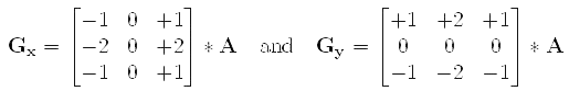
Gx = [f(x+1,y-1)+2*f(x+1,y)+f(x+1,y+1)]-[f(x-1,y-1)+2*f(x-1,y)+f(x-1,y+1)]
Gy = [f(x-1,y-1) + 2f(x,y-1) + f(x+1,y-1)]-[f(x-1, y+1) + 2*f(x,y+1)+f(x+1,y+1)]
G = sqrt(Gx^2+Gy^2)
Sometimes, in order to improve efficiency, we use an approximation of the above equation: |G| = |Gx| + |Gy|. If G is larger than a certain threshold, we then consider this pixel as an edge pixel.
Dilation and Erosion
Dilation and Erosion are two basic operators in Mathematical Morphology. They are typically applied to binary images. However, sometimes they can also be extended to grayscale images. For dilation, the effect would be gradually enlargement of the boundaries of the regions of foreground pixels. Thus areas of foreground pixels grow in size while holes within those regions become smaller. For Erosion, it is to erode away the boundaries of regions of foreground pixels (In our experiment, black pixels). Thus areas of foreground pixels shrink in size, and holes within those areas become larger. The two figures below show the different effects of Dilation and Erosion.
Dilation effect on Binary Images*
Dilation effect on Binary Images*
The dilation of A by B is defined as:
![]()
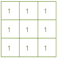
Here in our experiment, we are using a 3×3 square as structuring element, which is origin at its center. To compute the dilation of a binary input image by this structuring element, we consider each of the background pixels in the input image in turn. For each background pixel (which we will call the input pixel) we superimpose the structuring element on top of the input image so that the origin of the structuring element coincides with the input pixel position. If at least one pixel in the structuring element coincides with a foreground pixel in the image underneath, then the input pixel is set to the foreground value. If all the corresponding pixels in the image are background, however, the input pixel is left at the background value.
Similarly, the erosion of A by B is defined as:
![]()
Where Bz is the translation of B by the vector z.
To compute the erosion of a binary input image by this structuring element, we consider each of the foreground pixels in the input image in turn. For each foreground pixel (which we will call the input pixel) we superimpose the structuring element on top of the input image so that the origin of the structuring element coincides with the input pixel coordinates. If for every pixel in the structuring element, the corresponding pixel in the image underneath is a foreground pixel, then the input pixel is left as it is. If any of the corresponding pixels in the image are background, however, the input pixel is also set to background value.
Opening and Closing
Opening and Closing are another two important operators in Mathematical Morphology. They are usually applied to binary images. However there are grayscale versions as well. The basic effect of an Opening is somewhat like erosion in that it tends to remove some of the foreground pixels from the edges of regions of foreground pixels. However it is less destructive than erosion in general. Similarly, the basic effect of a Closing is similar to dilation in that it tends to enlarge the boundaries of foreground regions in an image and shrink background color holes in such regions, but it is less destructive of the original boundary shape.
The definition of Opening and Closing are both very simple. For Opening, it is defined as an erosion followed by a dilation, but using the same structuring element for both operations. For Closing, it is Opening performed in reverse, which is a dilation followed by an erosion using the same structuring element for both operations.
Simply speaking, the Opening is to break the small connections of different image parts, while Closing is to connect the small gap between different image parts.
High Level Design top
Rationale and Sources
There are many image processing methods are based on morphological algorithms. Actually, after doing morphological processes, we could realize many effects on the image being calculated. The morphology is usually based on binary images. However, if we do some minor modification of the algorithm and programs, it would be also applicable to grayscale images. That is one important part of our mission in this experiment.
In medical device industry, especially in medical image processing like CT, MRI, PET and even X-Ray, there is a lot of application of morphological methods. After discussing, we decided to build this process in real-time. That is to say, we need to develop fast and stable methods to collect data from the CCD, compute it, and finally display it on the VGA monitor. FPGA is high-speed and strong in parallel computation, so we choose FPGA to develop fast processing methods and algorithms.
Logical Structure
In our design, the whole system is built up with several modules, which is shown in the figure below. The video signal input feed is generated by the peripheral module TRDB-DC2 CCD camera provided by Bruce Land. With flat cable connected to DE2 main board, the video signal captured by CCD camera can be directly transferred to the DE2 board. However, the color profile of captured video is not RGB but another color system called Bayer. Therefore, the video signal will be decoded and transform from Bayer RAW to RGB colors. There is a sample project provided by Terasic DE2 CD-ROM. Inside it there is a RAW2RGB.v file that is used to transform the color system.

CCD Image Sensor Module Assembly
The video data is captured and input in real time and in pipeline path. The CCD Data Capture module will be used to give out the CLK signal to the CCD, and get back the serial data generated by the CCD camera. Also, the I2C_Controller will be controlling a set of parameters including the exposure, time delay, clock signal, etc. The signal is then transferred to color system transformation module to be decoded from Bayer Color Pattern System to RGB Color System. The standard 30-bit RGB data is generated. After that, the data is transferred into SDRAM to be stored and for following image processing steps. The 4-port SDRAM controller is the driver of on-board SDRAM. The RGB data as well as pixel data will be stored in SDRAM and then read out by the following VGA controller, to display on the VGA monitor at a resolution of 640x480.

High Level Logic Design
There is an Image Processing Module to take responsibility of all image processing algorithms and computations. This module reads data from SDRAM, computes the pixels as what we have initialed set up, and then transfer the data into VGA controller. The Image Processing Module consists of several sub-modules. The Edge Detection Sub-module will be calculating the edge using Sobel operator, and it has a 3- line buffer to make sure the reading of three lines at one time in order to improve the speed of the whole screen calculation. Using the Sobel operator in both vertical and horizontal direction, the Gx and Gy convolution is calculated by a Multiplier-Adder, and then added together by a Parallel Adder. Finally, the radication is done by a SQRT module, and if the result is larger than a certain threshold set by the toggle switch, it would be consider an edge pixel, and given a color black.
There are also parallel modules for grayscale image generation and binary image generation. The generated binary/grayscale and edge-triggered images will be used to show the morphological image processing. We have built Dilation module and Erosion module. For Dilation and Erosion, we can input the binary/grayscale image directly to the modules, and the output will be corresponding images. If we want to compute opening and closing, we can use the data from Dilation or Erosion module, and put it back to the other module to finish computing of opening and closing. For example, if we do an erosion followed by a dilation, then it would be opening. If we do a dilation followed by an erosion, it would be closing.
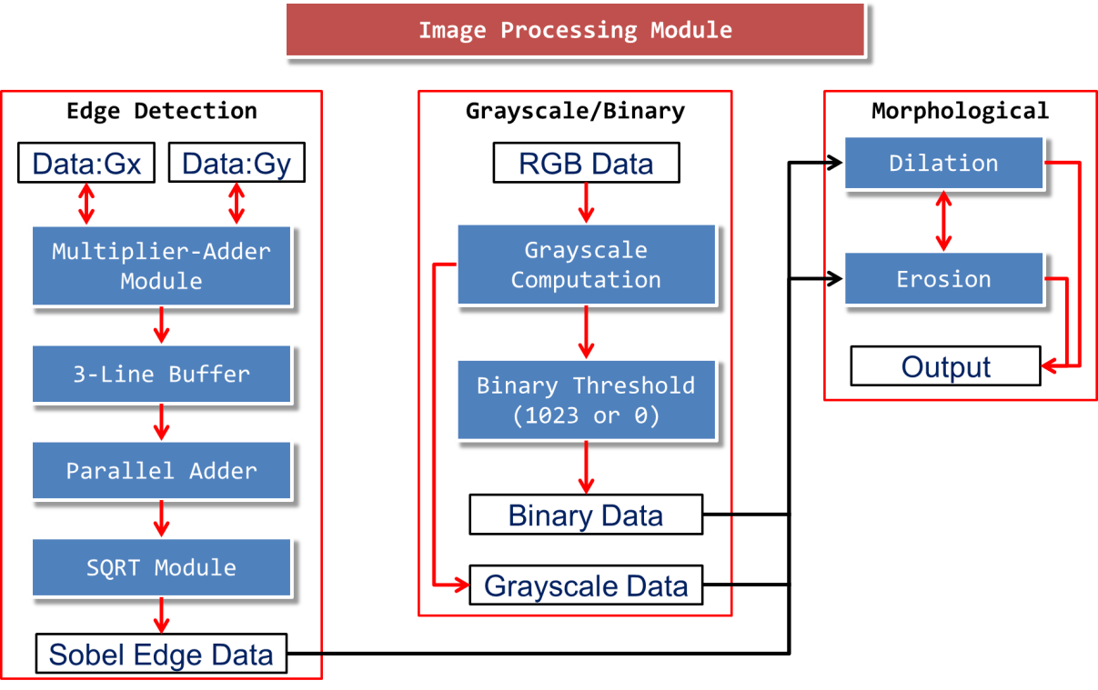
Image Processing Module
Trade-offs
The main trade-off in our project is the method we used for edge detection. We choose a simple edge detection algorithm of Sobel operator, since it always takes time to process the entire screen. If we choose other more complicated methods and algorithms, we might have crisper and clearer edges, but it would also takes much longer to compute the whole image. The more detailed edges we present, the more time taken to calculate. Also, more complex algorithms might cause problems in memory management, which is not what we would like to see during our experiment. Since we want to make the morphological image processing in real-time, which is the main goal of our final project, we decided to sacrifice some robustness and precision in order to gain higher speed.
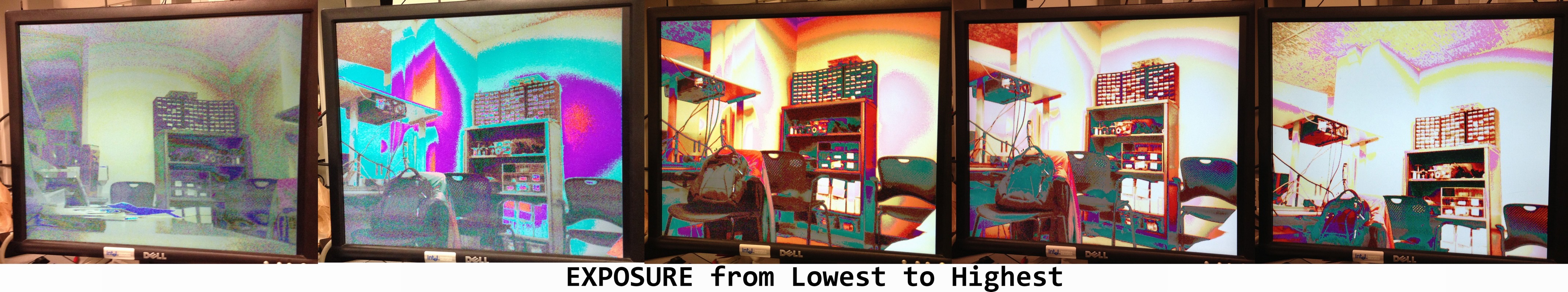
Another trade-off is the exposure adjustment controlled by the DE2 provided I2C_Controller. During our experiment, we met a problem that the exposure time of CCD cannot be adjusted by the toggle switches and KEY[1]. Also, there is a problem that when we press KEY[1] for many times, the VGA display will be in trouble: no more image, and half black and half white. We took quite a lot of pains to fix this bug, and finally we figured out the problem. Seeing from the simulation waveform scheme below, the LUT_INDEX has always been zero, and mSetup_ST has always been one. However, the corresponding I2C_ACK was displayed as high level while it was supposed to be low (low effective). So that is why the exposure time cannot be adjusted by toggle switches. After fixing the I2C_Controller, everything worked fine.
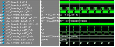
Simulation Waveform of I2C Controller
A minor trade-off is the manual adjustment of Sobel threshold, exposure threshold and morphologic image controller. There are only 18 toggle switches. However, as the DE2 sample project set, it used 15 toggle switches just to manually adjust the exposure time. That is definitely wasted a lot of toggle switches since the lower bit has little effect on the final exposure time result. In order to gain control of every function we presented in the experiment, as well as to get manual control of Sobel threshold and what morphological image to display, we deleted some toggle switches for exposure, and used definite “0” or “1” instead. The reserved toggle switches will only be controlling the higher bits of threshold which more significant to the final output results.
Hardware Resources Allocation
The Toggle Switch SW[17:0] functions are respectively defined as follows:

SW[17]: ON for Grayscale Image, OFF for Full Color Image;
SW[16]: ON for Sobel Edge Detection Mode;
SW[15]: ON for Binary Image Mode;
SW[14:12]: 000 for Binary Dilation, 001 for Binary Erosion, 010 for Sobel Dilation, 011 for Sobel Erosion, 100 for Grayscale Dilation, 101 for Grayscale Erosion, 110 for Sobel Closing, 111 for Sobel Opening;
SW[11:8]: Exposure time (Format: {3’b000, SW[11:8], 1’b0});
SW[7:4]: Binary Threshold (Format: {3’b000, SW[7:4], 3’b100});
SW[3:1]: Sobel Edge Detection Threshold (Format: {SW[3:1], 2’b10});
SW[0]: ON for morphologic image demo, OFF for normal image demo.
The Pushbutton functions are respectively defined as follows:
KEY[3]: Run;
KEY[2]: Freeze the capture;
KEY[1]: Apply newly set exposure time;
KEY[0]: Reset entire system.
The LEDs are set for indicating which toggle switch is in ON state, and which Pushbutton is pressed down.
The 7-Seg LED Displays are set to indicating elapsed time and frame rate.
Hardware top
From Bayer to RGB
The TRDB-DC2 CCD image sensor module uses a 1/3-inch megapixel CMOS active-pixel digital image sensor MT9M011. The MT9M011 pixel array is configured as 1316 columns by 1048 rows. The first 26 columns and the first eight rows of pixels are optically black, and can be used to monitor the black level. The last column and the last seven rows of pixels are also optically black. The black row data is used internally for the automatic black level adjustment. However, the first eight black rows can also be read out by setting the sensor to raw data output mode (Reg0x22). There are 1289 columns by 1033 rows of optically active pixels, which provide a four-pixel boundary around the SXGA (1280x1024) image to avoid boundary effects during color interpolation and correction. The additional active column and additional active row are used to allow horizontally and vertically mirrored readout to also start on the same color pixel.
![]()
Pixel Array Discription from Terasic Official User Manual
This image sensor uses a professional image profile and color format called “Bayer Color Format”. From the figure below, we could see that in this color format, the black pixels are set to zero. The even-numbered rows contain green and red color pixels, and odd-numbered rows contain blue and green color pixels. Even-numbered columns contain green and blue color pixels; odd-numbered columns contain red and green color pixels.
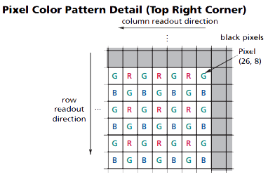
Pixel Color Pattern Detail from Terasic Official User Manual
Generally speaking, to convert the Bayer colors to RGB colors, we use the line buffer and pipeline processing mode. The line data of Bayer color pattern is captured in previous stage, converted to standard 30-bit RGB data and done with down sampling, in order to get fit for following image display.
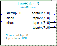
Firstly we call a megafunction called ALTSHIFT_TAPS. ALTSHIFT_TAPS can be used for data shift register group. The 3 taps of ALTSHIFT_TAPS will be used for a series of pixel data collected, and the width of each taps is the same as the number of pixels in a line, which is 640 in our experiment. During the format translation, we used for registers:
mDATA_0: The pixel of M row and N column.
mDATAd_0: The pixel of M row and N-1 column.
mDATA_1: The pixel of M+1 row and N column.
mDATAd_1: The pixel of M+1 row and N-1 column.
The four registers are combined together to generate a kernel template, in which the mDATA_0 is on the upper left:
| mDATA_0 | mDATA_1 |
| mDATAd_0 | mDATAd_1 |
In this template there will definitely be one R, one B and two G pixels. Therefore, the R is thought of as the R data for current pixel mDATA_0, B as the B data for the current pixel mDATA_0, and the average of two G pixels as the G data for the current pixel mDATA_0 (We simply take the upper 10 bits of G and ignore the last bit). For the entire image of Bayer color format, we pick up all the pixels of one color and implement the kernel template, then we will get the RGB color information and the conversion is done.
3-Line Buffer
The Three-line Buffer designed in our project is simply a series of 3 large registers built by MegaWizard Plugin Manager. The buffer is actually a RAM based shift register, and the RAM blocks type is M4K, which is optimized by the compiler. The registers are 640 pixels each line, and hold the pixel information for the entire line of the VGA screen. Each pixel has 30 bits of information, which consists of the color of Red, Green and Blue, 10 bits for each color. If the module is enabled, then on the clock edge our shiftin input will be stored in the first pixel of line1, with the rest of the pixels shifting up 1 slot. This pixel information is then later used in the top level module and output to the screen. We also output a grid of pixels, which are later used in our edge detection modules.
Multiplier-Adder
The Multiplier-Adder is also generated by MegaWizard Plugin Manager. There are three multipliers, and one adder used in the module. The bits of bus of both inputs are 8-bit, while the output is 18-bit. In the Sobel edge detection algorithm, the convolution is conducted as a series of multiplies and additions. As is shown below:
Gx = [f(x+1,y-1)+2*f(x+1,y)+f(x+1,y+1)]-[f(x-1,y-1)+2*f(x-1,y)+f(x-1,y+1)]
Gy = [f(x-1,y-1) + 2f(x,y-1) + f(x+1,y-1)]-[f(x-1, y+1) + 2*f(x,y+1)+f(x+1,y+1)]
The multiplier-adder module is linked to the 3-line buffer, and one of the inputs is from Line0 to Line2. The other inputs are the elements in the 3x3 matrix structure. This module will compute the parts of Gx and Gy, which will then be used in following modules.
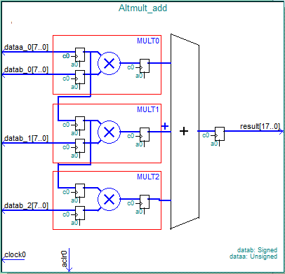
Parallel Adder & SQRT Module
The Parallel Adder is used in computation of Sobel operator. The result from Multiplier-Adder will be given into the Parallel Adder, and then be added together. The calculation is signed. After this step, the results of Gx and Gy will be finally computed out, and then given to following SQRT module.
The SQRT module is generated by MegaWizard Plugin Manager. It has a 32-bit input, and 16-bit output. The edge level G is calculated in this module. If G is higher than a certain threshold set by the toggle switches, then this pixel is considered as an edge pixel.
Grayscale Generation
To get grayscale image, we have to transform the RGB colors into grayscale. Generally speaking, a widely accepted method is to use the equation below:
Grayscale = 0.299 * R + 0.587 * G + 0.114 * B
However, such an equation definitely needs floating point calculation, which is not only hardware consuming, but also slow and low precision. It is slow even using C programming, not to mention Verilog. Sometimes people use another approximation of this equation:
Grayscale = (R + G + B) / 3
However, this method needs division, which is a little better than floating points, but also quite resource consuming as well. What’s more, it is not a formal transformation from RGB to grayscale, the image generated is lack fidelity.
Noticing that the weight of R, G and B are different, and the weight of G is almost twice as that of R, and 5 times as that of B. That is to say, the grayscale mainly lies on the level of G, but less on R and B. Therefore, we decided to use G level to represent the grayscale. This is also the best and fastest way to conduct such a transformation on hardware.
After the Bayer Color Pattern Data transformed to RGB data, the RGB color information takes over 30 bits in total. However, the grayscale is only 10 bits. Therefore we could save half the space on SDRAM, as well as half bandwidth. Here we cannot save 2/3 of total memory, because the WR1_DATA of SDRAM is 16-bit. While grayscale has only 10 bits, the rest of 6 bits are occupied by zero. From the SDRAM we give {Read_DATA1[14:10],Read_DATA2[14:10]}to Gray_G. The same data is also given to Gray_R and Gray_B.
Binary Image Generation
Binary image is fundamental for the following processing of other morphological images. To realize binary image, we will check every pixel of the entire screen to see whether it is beyond a certain threshold. If it is, then this point will be set to 1023 (10’b11111, 11111). If not, this point will be set to 0. In order to increase the speed of calculation and processing, we did not use the three RGB 30-bit color data, but simply use 10-bit grayscale information. In the binary image module, the input is the 10-bit grayscale data of each pixel, and the output is 10-bit 1023 or 0. Since in the official sample of DE2_CCD project there is a decoder to conduct traversal from the upper right pixel to the lower left one, we do not need to write a specific pipeline program to do the same thing.
The threshold of binary image will be manually adjustable by toggle switches SW[7:4], with a simple format of {3’b000, SW[7:4], 3’b100}.
Dilation and Erosion
To conduct dilation, for each background pixel we superimpose the structuring element on top of the input image so that the origin of the structuring element coincides with the input pixel position. If at least one pixel in the structuring element coincides with a foreground pixel in the image underneath, then the input pixel is set to the foreground value. If all the corresponding pixels in the image are background, however, the input pixel is left at the background value.
Similarly, to conduct erosion, we consider each of the foreground pixels in the input image in turn. For each foreground pixel we superimpose the structuring element on top of the input image so that the origin of the structuring element coincides with the input pixel coordinates. If for every pixel in the structuring element, the corresponding pixel in the image underneath is a foreground pixel, then the input pixel is left as it is. If any of the corresponding pixels in the image are background, however, the input pixel is also set to background value.
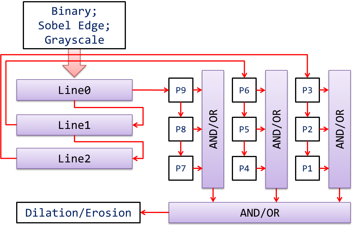
Logic Diagram of Morphological Image Calculation
Here we use a line buffer to do the AND or OR logic operation. The 3x3 square, which is considered as structuring element, is labeled for each cell from P1 to P9. Once it captured the signal of RST_N, which is given out by the VGA controller, the P1~P9 will be set to zero and ready for computation. For Dilation computation, when next clock pulse comes, the shift register will work, and every bit is shifted to left by one digit. For example, the Line0 is shifted to P9, P9 to P8, P8 to P7, Line1 to P6, P6 to P5, P5 to P4, Line2 to P3, P3 to P2 and P2 to P1. Then, if the iDVAL is high level, then it means this pixel should be dilated, which in our experiment is filled up with black. Otherwise the pixel is filled with white.
Similarly, for Erosion computation, the OR logic will be changed to AND logic, and the shift register and shifting operation remains the same. In the same way, if the iDVAL is high level, then it means this pixel should be eroded, which in our experiment is filled up with white. Otherwise the pixel is filled with black.
Results top
For our final results, we had a complete morphological image processing system that ran in real time. We could set the different kinds of threshold variably, including threshold of binary image, exposure image and sobel image. Right now we could display in binary image, grayscale image. And we could also realize the basic morphological effect of Dilation, Erosion, Opening and Closing. We accomplished the goals that we set out, and the video output looked like what we expected.
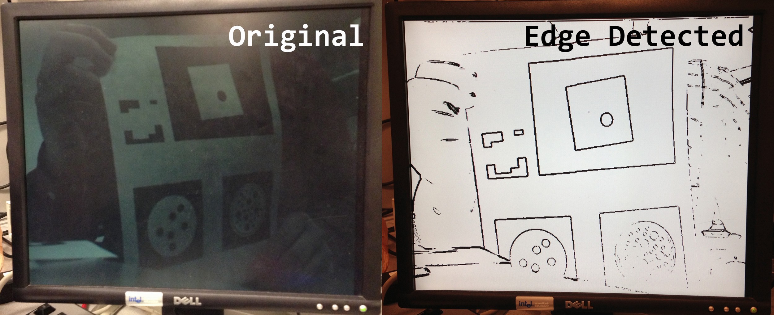
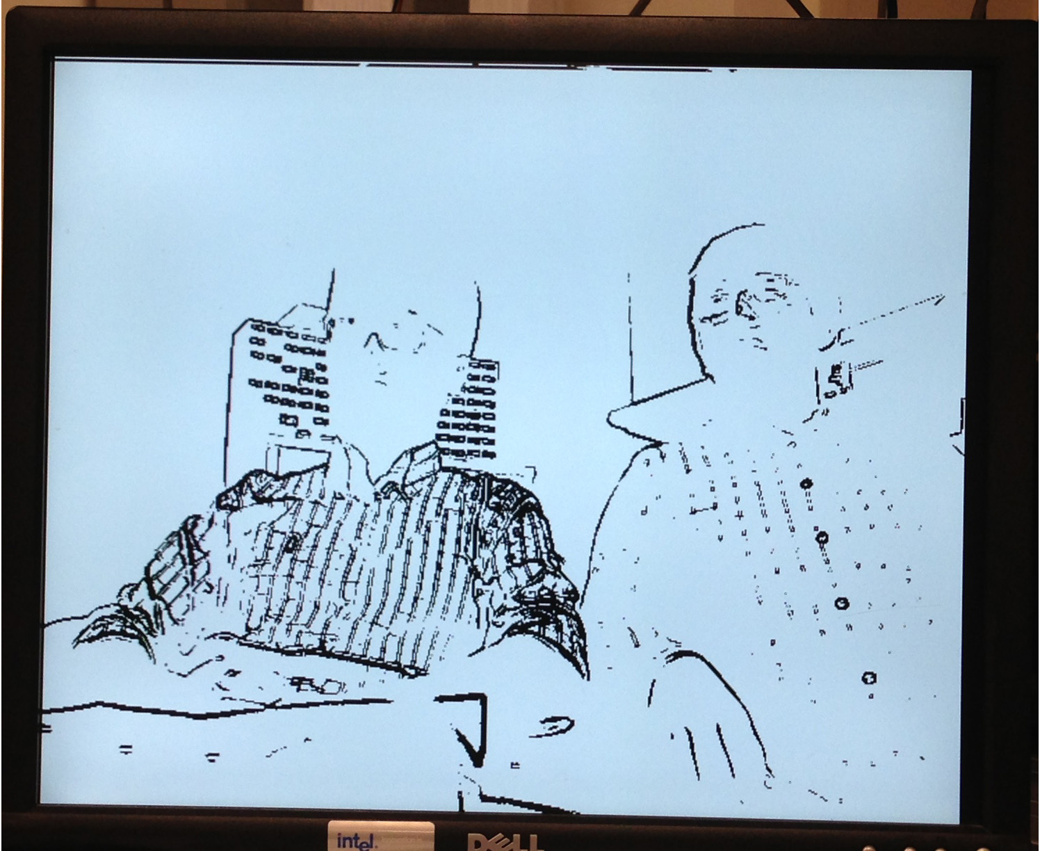
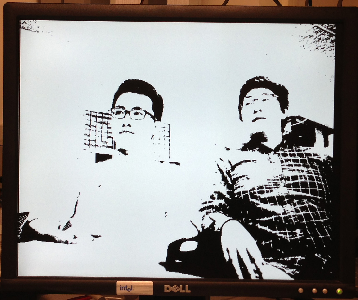
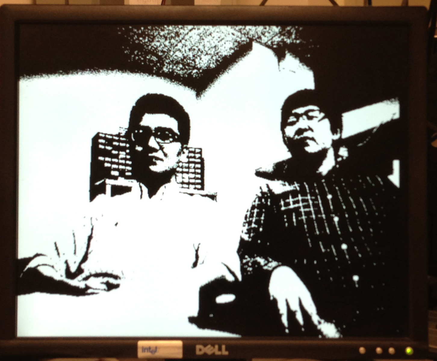
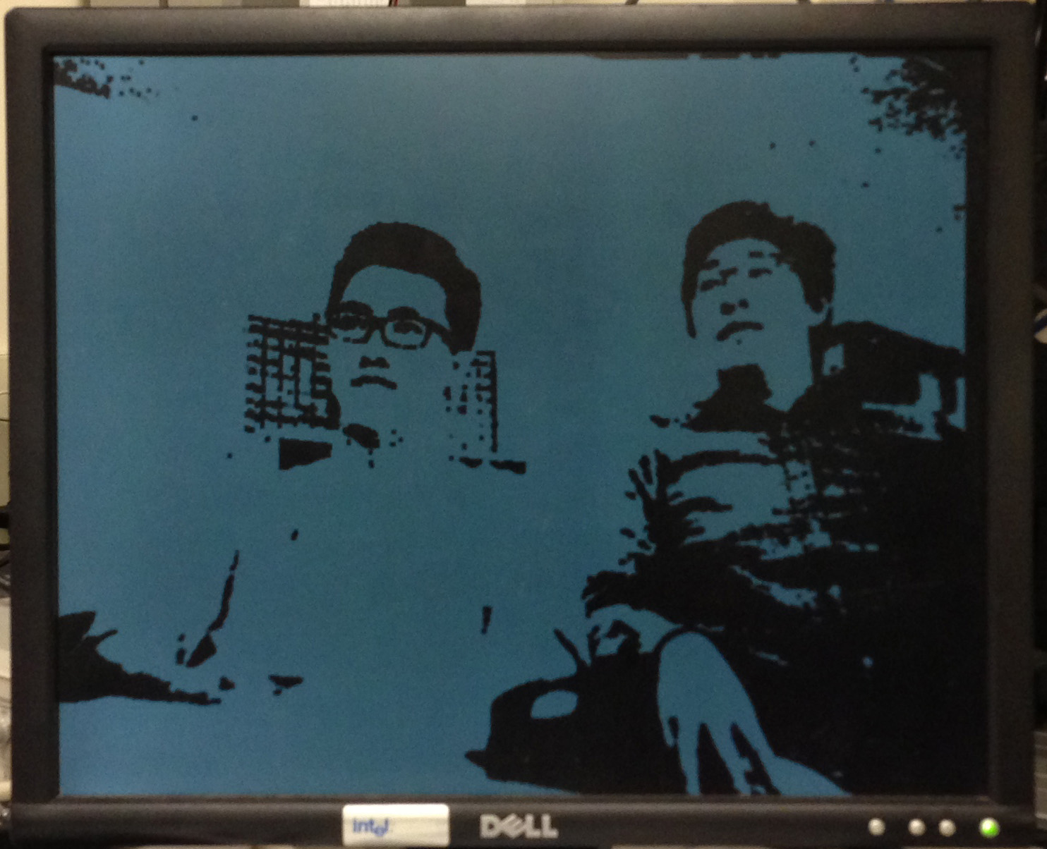
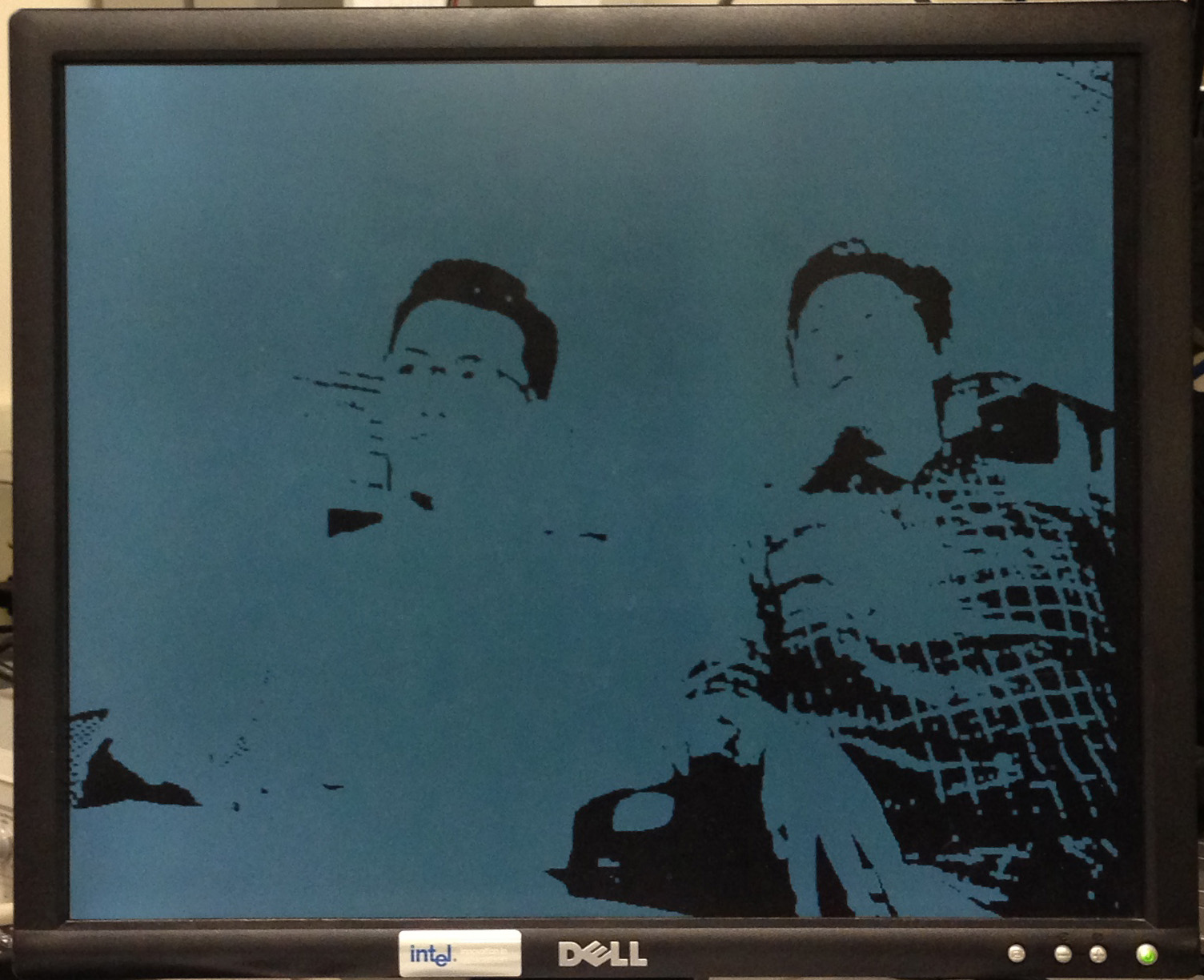
We have attached two sample images from our output. One is the Rage Comics Effect generated by Binary images. The other is a demo of original image and its Opening image. There are additional photos in the Appendices.
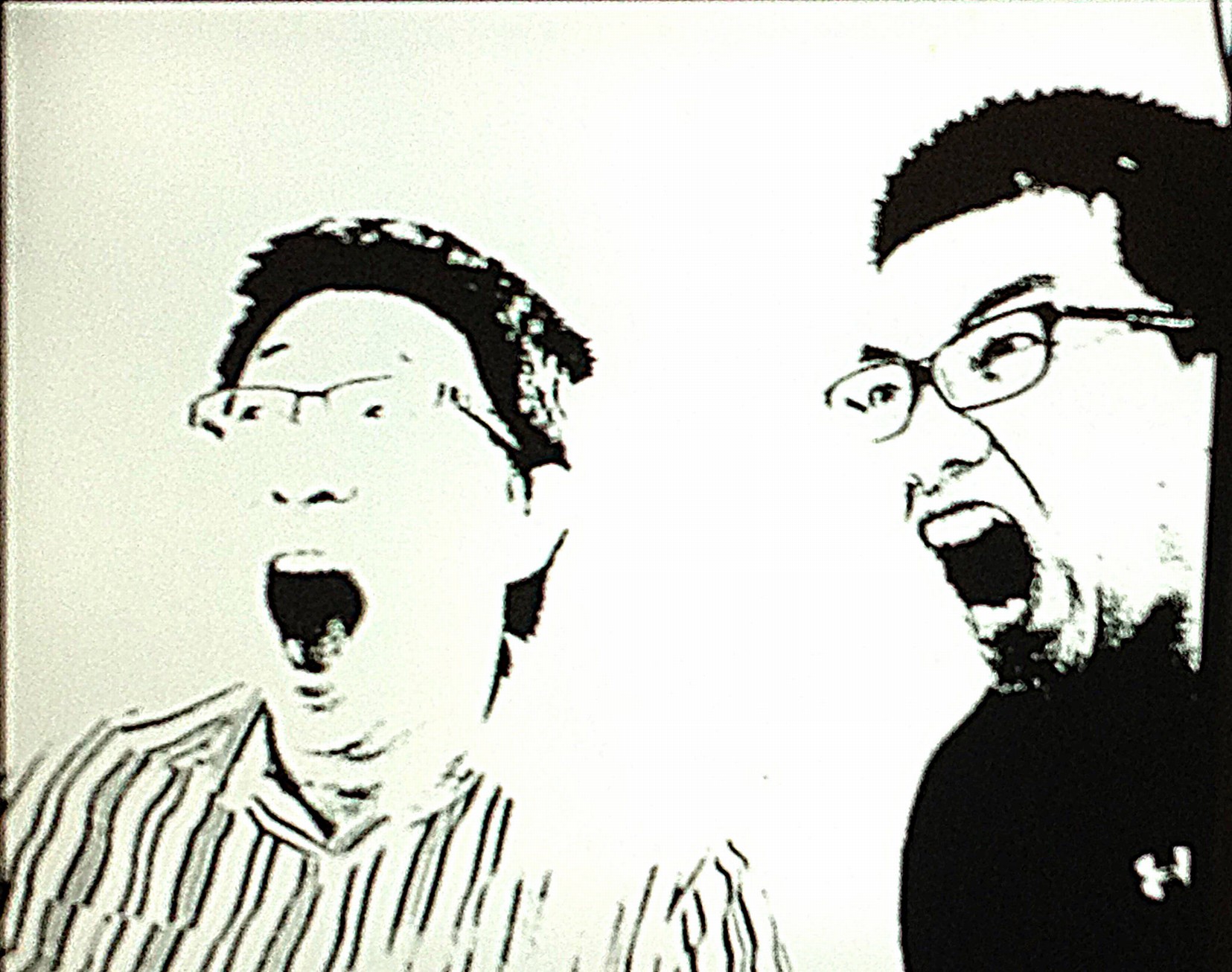
Binary Rage Comics Effect
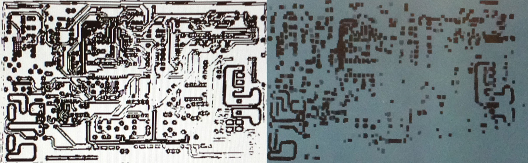
Original image and its Opening image
Conclusions top
We got satisfied with our result of the project. We have a created a FPGA based real-time Morphological Image Processor. The image we produce are pretty nice and to some extent they could be treated as very nice sketches. The noise has also been filtered clearly when we choose higher threshold which could get even higher definition on all the edges. We were able to accomplish all of this while keeping the hardware fast enough to keep up with the constantly updating stream of video data from camera Terasic TRDB-DC2.
We got five mathematical morphology function on the FPGA but In fact, the total resource we use on the FPGA board is quite small. When looking through the report generated after compiling the code, we saw we use 9% of the total logic elements, which includes 7% of total combinational functions and 6% Dedicated logic registers. These modules are very compact and concise so that we may utilize the rest of them in our future work.
However, we were not able to produce ideally gradient images and we also have difficulty in producing exactly precise opening and closing operation. The reason for the gradient image is that when it comes to the pixels that need not change, we just simply give a zero or 10'd1023 to it. That leads to the total white or total black of some specific pixels, like some edge or a big piece of areas with same color. The reason for none-perfect opening and closing function is that we sacrificed some precision and simplified the algorithm in order to guarantee calculation speed.
The project is quite interesting and it challenged us in video processing, real-time calculation, and embedded system design. A large portion of it is based on the Terasic example code (DE2_CCD) that came with the DE2 board, we have added individual modules for specific task. This platform is easy for us to implement our future ideas on real-time image processing.
Appendices top
A. Experiment cost details
The DE2 Development board we used was generously donated by Altera, and the TRDB-DC2 CCD Image Sensor was lent to us by Bruce Land. Any other resources used, such as VGA cables and monitors were provided in the lab.
B. Source Code
The programs file capsulated in sof binary format is available here: DE2_CCD.sof.
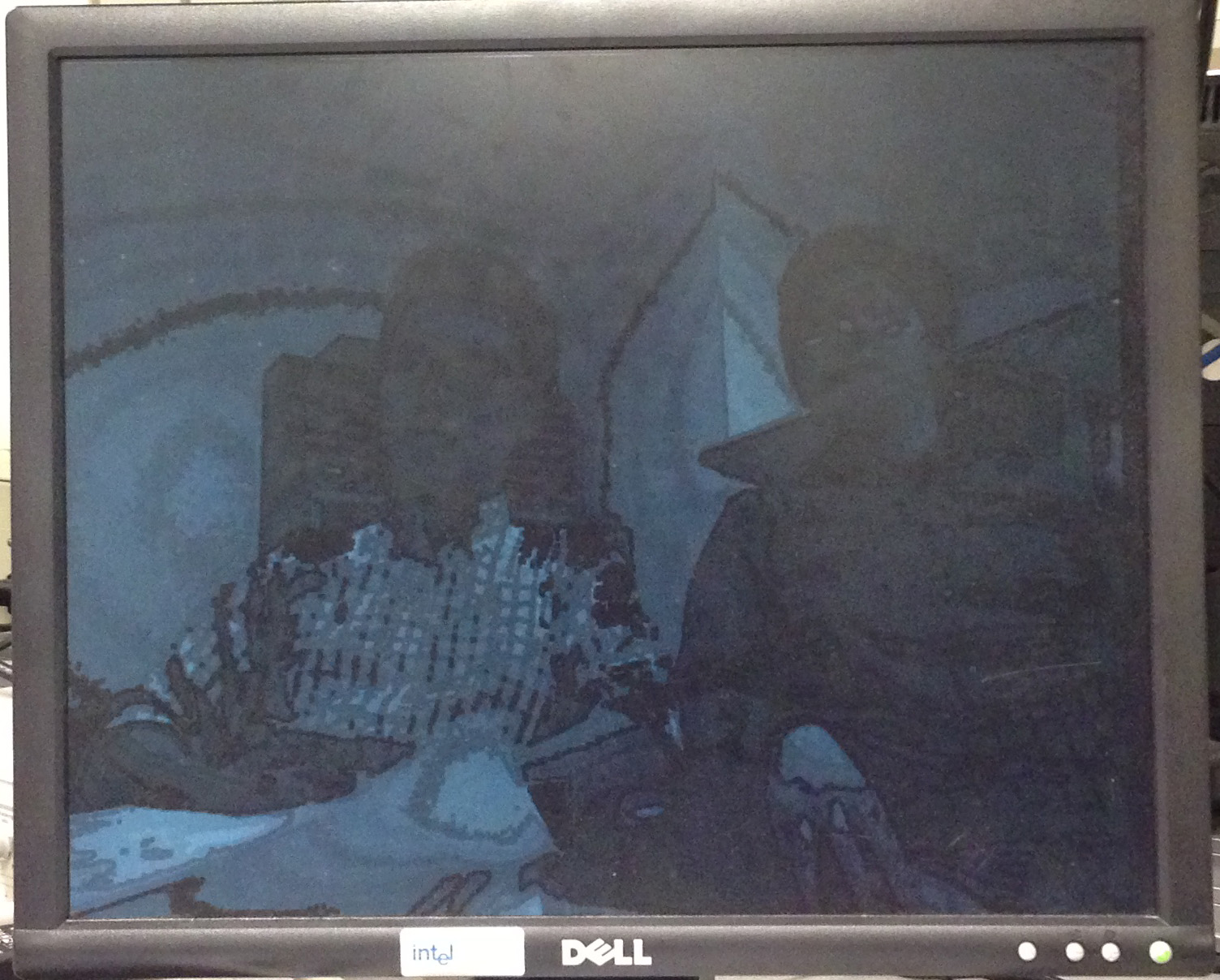
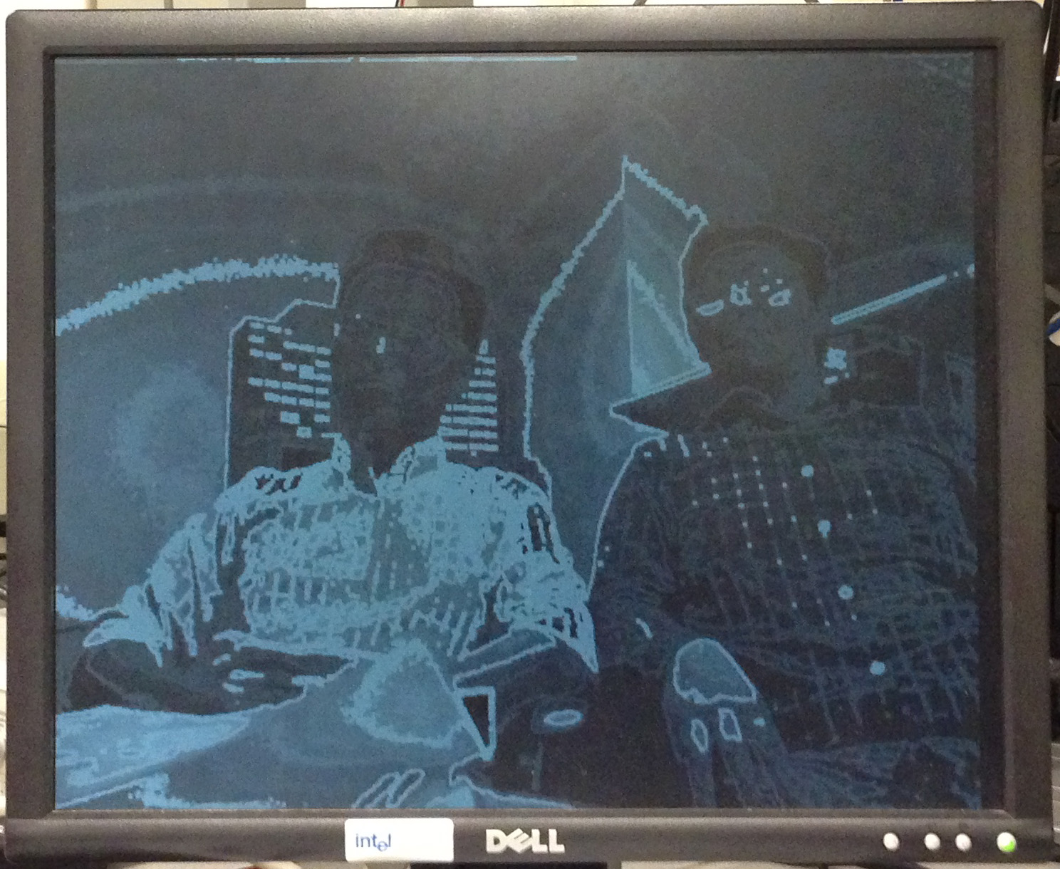
C. Photos of Results
D. Specific Task Breakdown
| Xiaofan Bao | Both | Jiayuan Wang |
|---|---|---|
| High level logic and system design | Hardware Testing | CCD peripheral implement |
| Grayscale/Binary Image generation | Debugging | Sobel algorithm design |
| Morphological algorithm design | Website content | Edge detection modules |
| Morphological modules | Photograph taking and graphics | Website formatting |
References top
We referenced much of Bruce Land's lecture material, especially with regards to edge detection schemes. We also used the CCD Decoder module provided by Terasic, from a CD-ROM which came with the DE2 Development Board. We referenced a few websites and data sheets for general background information, including our morphological image processing algorithm, which are listed below.
Datasheets
Vendors
References
Acknowledgements top
We would like to thank our friend and instructor, Dr.Bruce Land to help us in countless ways in hardware design, programming, and how to debug our program. We learned the principles of Verilog, the memory usage and control such as SRAM, SDRAM, the VGA display, and parallel computation, etc. Thanks him to teach us the whole semester with the FPGA knowledge. And We would like to thank our TA, Annie, too. She also helped us with our debugging and some strange problems we met during our experiment.
We would like to thank Altera for donating the DE2 FPGA boards to Cornell University for us to use. We would also like to thank Terasic for their example code, specifically the SDRAM Controller, VGA Controller and CCD Video Decoder code.
Team Members top
 |
Xiaofan Bao
M.Eng Student, 2012
Biomedical Engineering
Interests:
Hardware Engineering, Embedded System, Medical Instrumentation and Devices
|
 |
Jiayuan Wang
M.Eng Student, 2012
Electrical and Computer Engineering
Interests:
Hardware Engineering, Embedded System, Wireless Sensor Network
|