ECE 5760 Cornell University

Introduction
Nakano, K., et.al.(refs below) describe two versions of a small stack machine suitable for implementation on an FPGA and they give the Verilog source code on their web site. The design was ported to the DE2 board and extended to have a richer set of opcodes and i/o ports. I wrote a simple assembler and compiler for the architecture and implemented serial communication routines. The compiler supports inline macros, functions, one dimensional array variables, and the usual if-then-else-endif and while-do-endwhile structured programming. Supplied functions allow you to send and receive integers to the serial interface and to send strings and integers to the LCD..
CPU
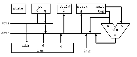
The cpu is a stack machine. The registers are arranged in a stack with the usual range of arithmetic operators and stack manipulation instructions. There are no named registers except top-of-stack (named top) and next-to-top-of-stack (named next).
The CPU design is from http://www.cs.hiroshima-u.ac.jp/~nakano/wiki/ and is GPL licensed. I added load/store opcodes and program counter push/pop. Load and store enable register indirect addressing, while PC manipulations enable functions. The single cycle version with a stack size of 16 occupies about 1100 logic elements (out of 33,000 on the DE2). Reducing the stack size to 8 drops the size to 940 logic elements. Setting QuartusII to optimize for speed (See Tools...Advisors...Timing optimization advisor) increases size to 1000 logic elements and increases the operating frequency to 74 MHz.
The cpu was extended to allow for up to eight in/out ports, with four appearing outside the cpu module. I/O addressing is shown in the opcode table below. The remaining four will be used for internal i/o, perhaps with a timer peripheral. The architecture taken from Nakano, K., et.al is shown below, but modified for 8 i/o ports and with an extra connection from the PC to the data bus (dbus).
CPU opcodes and instruction format
The cpu instruction set is shown below. Notation:
I is a 12-bit signed integerA is an unsigned 12-bit integern is a 3 bit integer (used only as an i/o address)top is top-of-stacknext is second-to-top-of-stackPC is the program countermem[A] is the contents of memory location A.| Instruction | Hex format | Operation |
|---|---|---|
nop |
0000 |
none |
pushi |
1000 + I |
[sign extended] I → top |
push A |
2000 + A |
mem[A] → top |
pop A |
3000 + A |
top →mem[A] |
jmp A |
4000 + A |
A → PC |
jz A |
5000 + A |
if (top==0) then A → PC |
jnz A |
6000 + A |
if (top!=0) then A → PC |
ld |
7000 |
mem[top] → top |
st |
8000 |
top → mem[next] |
pushpc |
9000 |
program counter → top |
poppc |
9001 |
top → program counter |
in n |
d00n |
input[n] → top |
out n |
e00n |
top → output[n] |
add |
f000 |
next + top → top |
sub |
f001 |
next - top → top |
mul |
f002 |
next * top → top (in 10.8 fixed point) |
shl |
f003 |
next << top → top |
shr |
f004 |
next >> top → top |
band |
f005 |
next & top → top |
bor |
f006 |
next | top → top |
bxor |
f007 |
next ^ top → top |
and |
f008 |
next && top → top |
or |
f009 |
next || top → top |
eq |
f00a |
next == top → top |
ne |
f00b |
next != top → top |
ge |
f00c |
next >= top → top |
le |
f00d |
next <= top → top |
gt |
f00e |
next > top → top |
lt |
f00f |
next < top → top |
neg |
f010 |
-top → top |
bnot |
f011 |
~top → top |
not |
f012 |
!top → top |
dup |
f013 |
copies top of stack -- stack: top → top top |
drop |
f017 |
drops top of stack-- stack: next top → next |
over |
f01f |
copies next to stack top -- stack: next top → next top next |
dnext |
f01b |
drops next -- stack: next top → top |
See this page for older versions and develpment sequence.
Simple Compiler (Syrup)
A simple compiler, named Syrup, was written in matlab (also runs in Octave) to make programming easier.
A source code is assembled into a mif file, which can be read by the ram block. The link between the mif file and the Pancake cpu ram block is implemented with a synthesis directive in the same statement as the memory declaration and before the semicolon which terminates the declaration.
reg [DWIDTH-1:0] mem [WORDS-1:0] /* synthesis ram_init_file = " test_stack_machine.mif" */ ;Search for
/* synthesis ram_init_file in the verilog file containing the cpu and modify the mif name.
If you change the mif file by recompiling (but keep the mif file name the same), then you can change the memory contents without having to rebuild the whole project:
(1) Click Update Memory Initialization File on the Processing menu.
(2) After using this option, run the QuartusII Assembler (Processing menu...Start...Start Assembler) to generate new programming files for the device.
The compiler_v1_12 syntax is stack based and written in Matlab (version 1.0). A description follows:
constant keyword.constant
key3mask 8
; name -- value pair
redLEDs 3 ; port 3 variable keyword. Examplevariable
test ; define a 1 word variable
particle 100 ; define array of length 100 inline keyword. inline/endinline. inline
inc
1 add
endinline function keyword. function
getchar
putchar
delay_10
puthex program keyword. Example:program ; this section contains the actual program main: 0 =count ; loop forever waiting for human input while forever ; never exit do "enter> putstr gethex crlf puthex space count puthex crlf count 1 add =count endwhile ; end of infinite loop
main: . redLEDs key3mask add =test puts the value 11 into the variable test. var1[var2] treats var2 as an index into var1 and places the value of the indexed variable on the stack. =var or =var1[var2] stores the value on the stack to the appropriate location. count by pushing the memory value onto the stack, pushing 1 onto the stack, adding them, and popping the stack back into memory.count 1 add =count
add, sub , shl, shr, band, bor, bxor, and, or, eq, ne, ge, le, gt , lt, neg , bnot , not, drop, over. "string places the string on the stack (with a character count) to be printed by putstr (see below). "enter> places the characters enter> on the stack with the e at next-to-top of stack and the character count at top-of-stack..putstr. in[const] and out[const].redLEDs defined above out[redLEDs]funct_entry: funct_entry. The exit point of a called function is indicated by return. inline make_vga_addr
8 shr 9 shl =temp
8 shr temp add
endinliney[count] x[count] make_vga_addr out[vga_addr] if then else endif. if x[count] 480 gt
then 478 =x[count]
endifwhile do endwhile. counter2 to zero and increments the counter until it overflows.while counter2 0 ne
do counter2 1 add =counter2
endwhile opcode.operand or opcode. if there is no operand.
inline swap

      pop.4 ; locs 4&5 are hidden temp locations

      pop.5

      push.4

      push.5

      endinline
The compiler generates code to initialize the return stack and then jumps to main.
Code starts executing at memory location zero, but your program starts at main:.
The return stack is allocated in high memory, with variables just below. There is no collision detection between code and variables.
Note that the parser is really stupid! No are spaces allowed between equal sign and variable name. No spaces allowed in indexed variable syntax.
Compiler wish list: Local variables, nested inlines, "include", variable/array initialization, ashr (arithmetic shift right), mul and fixmul
Compiler Example
A short example shows how to blink LEDs using this hardware design. It shows the five basic sections of a program:
; This program demos compiler
; with LED output and button input
; ==================================

constant ; named constants
	key3mask 8
	key2mask 4
	keys 1  ; port 1
	keymask 15 ; 0x0f
	pattern2 255 ; 0xff
	pattern3 15 ; 0x0f
	redLEDs 3 ; port 3
	greenLEDs 2 ; port 2
	forever 1 ; endless loop

; ==================================

variable
	test   ; location to push test data
	counter1   ; outer loop counter
	counter2   ; inner loop counter

; ==================================

inline inc
	1 add
endinline

; ================================

function
	evalkey

; =================================
program ; this section contains the actual program

main:
0 out[greenLEDs]; reset the green LEDs
0 =counter1 ; init counter

while forever ; never exit
do
	counter1 inc ; get the counter and increment
	dup ; copy stack top
	out[redLEDs] ;output one copy, one on stack to store
	=counter1  ; save the counter

	;slow it down with an inner loop counter
	1 =counter2 ; reset and store inner counter
	while counter2 0 ne ; compare stack top to zero
		do counter2 inc =counter2 ; inc the counter
	endwhile	;end of inner loop

	; detect some button presses
	if ; is KEY[3] pressed?
		key3mask evalkey ; detect 4th bit set
	then ; key 3 is pressed
		pushi.pattern2 out.greenLEDs
	else ; key 3 is not pressed
		pushpc.  out[greenLEDs]
	endif
endwhile ; end of outer loop

;=== read keys function ====
; enter with a switch selector bit on the stack
; exits with a TRUE/FALSE for match/nomatch on stack
evalkey:
	in[keys] bnot ; invert so key-down==1
	keymask band ; use only lower 4 bits
	eq ; compare to specific_keymask
	return

;===end of code ============================
Serial input/output
I used serial hardware from John Loomis (see ref below) to add i/o to the stack cpu. The serial i/o will work up to 115200 baud, but is set in the example to 9600 baud. Connection was made to the PC from the RS-232 connector on the DE2. The PC is using the terminal emulator PuTTY, but you could use serial input to Matlab also. The top level module has the serial routines included, but be sure that the mif file name in the memory module matches that generated by the compiler. The source code implements the low level interface routines getchar and putchar, then uses them to build putstr, gethex and puthex. Gethex and puthex read and write a single 18-bit number to/from the stack. The main routine prompts the user to enter a number, then prints it, along with a sequence number. The code as implemented assumes a clock frequency of 50.4 MHz. You can change that in the RS232 modules. Zipped project.
Serial input/output and LCD output
More hardware from John Loomis (see ref below) was used to add LCD output to the stack cpu. I modified the structure of his controller for serial character writing and to make the LCD reset a little more robust. The top-level file contains the spu definition the RS232 routines and the LCD routines. The compiler source code implements LCD reset, clear, putstr and puthex commands. When you modify the code, be sure that the mif file name in the cpu memory module matches that generated by the compiler. Zipped project.
Graphics examples
The processor was hooked up to the VGA display using M4K blocks, with one output port for address, one port for 1-bit data and one port for write-enable. A software 36-bit. linear feedback, shift register random number generator produces random single bits to simulate diffusion with 1800 particles. The computational frame rate is 75 fps with 1800 particles, running at the VGA clock frequency of 25.2 MHz. The timing analyser says that the cpu should run at 67 MHz, but it seems to run at 75.6 MHz, updating particle positions at 224 fps with 1800 particles, however, the video display wavers a little. At 50.4 MHz, 150 fps, the display is fine. The source code shows a longer computational example. The temporary asm file and mif file show the steps in getting the source code to the processor. Zipped project.
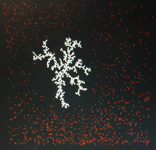
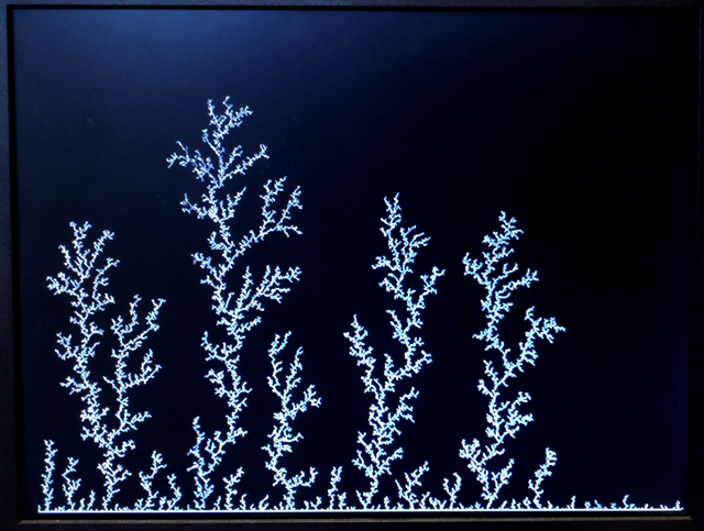
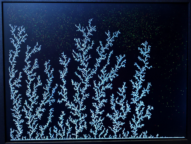
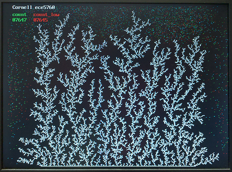
The fast processor was hooked up to SRAM to control the VGA. The interface was arranged so that the VGA controller runs SRAM, except when VGA_BLANK is asserted (low). The source code has to detect and respect the status of VGA_BLANK, only doing read/write when VGA_BLANK is low. The application computes a diffusion-limited aggregation. One thousand particles (in red below) are animated from cpu RAM, but collisions between the 1000 particles and the growing aggregate (in white below) are detected by reading back the position of aggregate particles from VGA SRAM. This means that the size of the aggregate is not limited by cpu memory, but only by the number of pixels on the VGA display. (hardware, source). A change in the source starts from a linear seed along the bottom of the screen. (hardware, source, zipped project). The image shown to the middle has about 8000 particles in the tree-shaped white aggregates. Inlining the random number generator and eliminating the animation of the diffusing particles (and showing only the aggregate) speeds up execution by several times (source). The right hand image has about 12,000 particles.

Multiprocessor graphics
Three fast processors were hooked up to SRAM to control the VGA. A hardware SRAM memory multiplexer was built to give priority to reset, then to the VGA controller, then each of the three cpus. The source code has to signal that it wants SRAM access, then wait for SRAM available, then read/write and then signal completion.
In the first pass of the design, SRAM access takes seven cpu cycles for a read or write because of sync overhead in the source code. Each cpu can only read/write when VGA_BLANK is asserted. The application computes a diffusion-limited aggregation with 1000 particles per processor colored in green, yellow and cyan on the screen. The image shown below-left has about 20000 particles in the tree-shaped white aggregates. All three cpus run the same code, with one input used to set the cpu id number. (hardware, source, zipped project). The image in the middle has about 36,000 particles in the aggregate (source) took about 6 minutes to compute.
In the second pass of the design, SRAM access is interleaved between the VGA controller and the three cpus. The VGA controller gets access on every VGA clock high, while the cpus share every VGA clock low. This works becuase memory is being clocked twice as fast as the VGA clock. On every VGA clock high, an address is set up based on the VGA address generator. On the VGA clock low, the SRAM data for the VGA is buffered into a register, while the address for the cpu read/write is set up. On the next VGA clock high, the SRAM data is buffered into a register for each cpu, while the next VGA controller read is set up. Execution time for the code speeds up by a factor of five for 1200 particles on each cpu producing an aggregate of around 32,000 particles (hardware, source, zipped project).
A ROM character generator for VGA was built, based on the data from ECE 320 at BYU. The file from BYU is here, and the matlab program to convert it to an Altera mif file is here, and the mif file is here. The ascii character code is multiplied by 16 to from the base index for a character. The data at the base index location is the top byte (of 16) of the character image. The high order bit of the byte is the left-most pixel of the top line of the character. The ROM was connected to i/o ports on the stack processor, cpu 1, where a small routine reads the ROM and outputs colors to the VGA SRAM interface. (hardware, source, zipped project)


The SRAM interface to the VGA display actually has over 100,000 unused bytes which are not displayed, but the unused memory is in small chunks. The biggest piece of available memory is from address 246,400 to 262,144, or about 16 kbytes. These unused locations can be used to share non-graphics data between processors. We need 16-bit read/write functions and a mutex to lock memory. The SRAM switch used in the graphics functions above was extended with new functions to allow 16-bits to be written (the graphics interface writes only single bytes). The mutex is implemented using hardware test-and-set, clear, and read instructions. The hardware switch prioritizes memory access first, then mutex operations. On the processor side, the program must: (1) set up an sram read, write, or mutex operation, (2) assert a request, (3) wait for access achnowledgment, (4) do the read/write (5) de-assert request. The test program computes a diffusion-limited aggregation, as above, maintains a shared (mutex protected) count in sram, and maintains a shared run/done flag in sram. (hardware, software, zipped project). And a video of the aggregate growth. The image below shows two counters in the upper left. The green counter is from shared, mutex protected memory. The red counter from shared, unprotected memory. The unprotected count is almost always lower than the protected count because of rare (but inevitable) overlap of two cpus trying to update the count at the same time. Another set of mutexes guarantees that cpu 2 and 3 will finish before cpu 1 tries to print the final count. It does this by setting a lock for cpu 2/3, then having each cpu clear its lock when it finishes.
The processor interface to the memory switch uses several i/o ports:
The control word on out2 has the following format. The 4 request lines are mutually exclusive.
The seven functions to access shared memory/mutex are written as inline functions described in the table below. The test-and-set operation on a mutex is atomic. It is guaranteed that if two cpus both try to set a mutex at the same time, only one will succeed, and they both will agree which one has set it.
| function | input stack | output stack |
effect |
vga_point |
color y x (stack top) |
-- |
Draws a point on the VGA display at (x,y) |
vga_read |
y x |
color |
Reads the 8-bit color of a point on the VGA display. Color code is explained in the hardware. |
sram_write |
data addr |
-- |
Writes a 16 bit word to SRAM addr |
sram_read |
addr |
data |
Reads a 16 bit word from SRAM addr |
mutex_test_set |
mutex_number (0 to 7) |
mutex_state (before setting) |
Reads a mutex then sets it, if it is zero |
mutex_clear |
mutex_number (0 to 7) |
-- |
Clears a mutex to zero |
mutex_read |
mutex_number (0 to 7) |
mutex_state |
Reads a mutex state (1/0) |
Slower, but smaller, multicycle version
This version of the processor (top_level, cpu_pll) has the same instruction set architecture and runs code (test1.cmp) using the same compiler (version 1_11), but uses half the memory and about 80% of the logic elements. The processor cycle speed is 100 MHz, but the average instruction takes a little over 3 cycles, so the processor runs at about 30 MHz. To enable the design to run at 100 MHz, you need to optimize Quartus for speed using the timing advisor.
Connecting this slower processor into the M4K-based VGA video circuit and running the diffusion source code results in a frame rate of 78 frames/sec with 1800 particles and the cpu clocked at 94 MHz. Only binary color is available because of limited M4K blocks. Zipped project.
 I wanted convert the graphics examples to SRAM-based VGA circuitry to allow more colors. This top-level module, running this source code, produces a color display with 8-bit color and a user definable hardware color map. If the cpu respects VGA timing the 307,000 pixels take 2.5 seconds to write. Ignoring VGA sync allows a full screen write in about 300 mSec, but results in video noise. Zipped project. Red and green each have three bits of intensity, while blue has two. Format is red encoded by bits 7:5, green by bits 4:2, blue by bits 1:0.
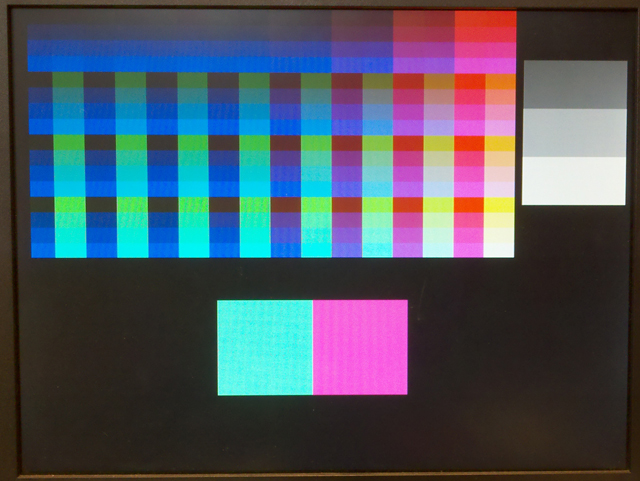 I modified the color map to enhance the red channel and rearranged the color display to patches showing colors and gray scale. At the bottom of the screen are two patches which have color set by SW[15:8] and SW[7:0] respectively. (top-module, source, zipped project)
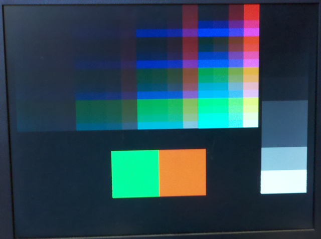 Another modification to the colormap encodes intensity in two bits, and r, g, and b in two bits each. (top-module, source, zipped project). The map has a larger intensity dynamic range, good saturation at high intensities and a more natural order. With the cpu clock set to 94 MHz, there was a tendency for the video to quiver a bit at high intensities. Setting the cpu clock to 50.4 MHz fixes the quiver.
Earlier versions and developmental sequence.
References:
Nakano, K.; Ito, Y., Processor, Assembler, and Compiler Design Education Using an FPGA, Parallel and Distributed Systems, 2008. ICPADS '08. 14th IEEE International Conference on; 8-10 Dec. 2008 pages: 723 - 728 (Nakano, K.; Ito, Y.; Dept. of Inf. Eng., Hiroshima Univ., Higashi-Hiroshima, Japan)
Nakano, K.; Kawakami, K.; Shigemoto, K.; Kamada, Y.; Ito, Y. A Tiny Processing System for Education and Small Embedded Systems on the FPGAs, Embedded and Ubiquitous Computing, 2008. EUC '08. IEEE/IFIP International Conference, Dec. 2008 pages: 472 - 479
John S. Loomis, Digital Labs using the Altera DE2 Board, http://www.johnloomis.org/digitallab/, Electrical and Computer Engineering, University of Dayton, Dayton, OH 45469-0232
Copyright Cornell University
March 11, 2013
Bruce Land