Verilog Summary
Cornell ece5760
Verilog Design
Verilog is one of several languages used to design hardware. It uses a C-like syntax to define wires, registers, clocks, i/o devices and all of the connections between them. Every useful Verilog design will include some sort of state machine(s) to control sequential behavior. We will be using only synthesizable Verilog-2001, except for simulation testbench code. What I want to do here is mostly to list some resources and some things to consider when writing Verilog.
Some other resources:
Verilog looks like C but it is quite different:
- Since we are assigning voltages to wires, which each must always have a logic level, the language is inherently parallel.
- Every assign statement happens all the time. And see below for two different assignment operators.
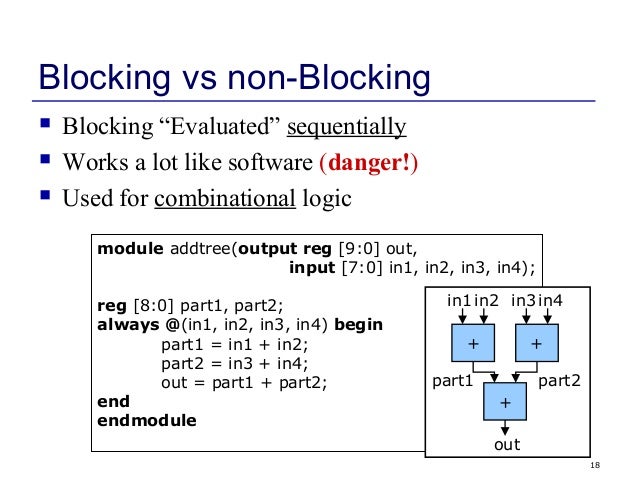
- Inside an always block (using blocking assign), statement order infers logic structure not sequential execution!
- Order of assignments is largely arbitrary -- make it readable!
- C is sequential because someone built a state machine that enforces sequential fetch-execute logic from a program location.
In Verilog, you have to build your own state machine, if you want any sequential actions to occur.
- Synthesized Verilog code is mapped to actual gates, not to abstract bit strings in computer memory.
- Timing is determined by physical hardware, not delay notations used in simulation, or by any clock, unless in a clocked always block.
- Module invocation implies building hardware connections, not a function call.
This implies that you cannot instatiate a module in an always block.
- Syntax has hardware consequences!
- Each plus sign instantiates a new adder.
Grouping add operations into a tree will change timing, therefore operations do not completely commute.
- Each multiply uses a DSP block (unless you surpress it).
- Loops build copies of hardware, not sequential actions.
The only sequential construct is a clocked state machine!
Use a generate statement to control looping, page 21 in Verilog Guide
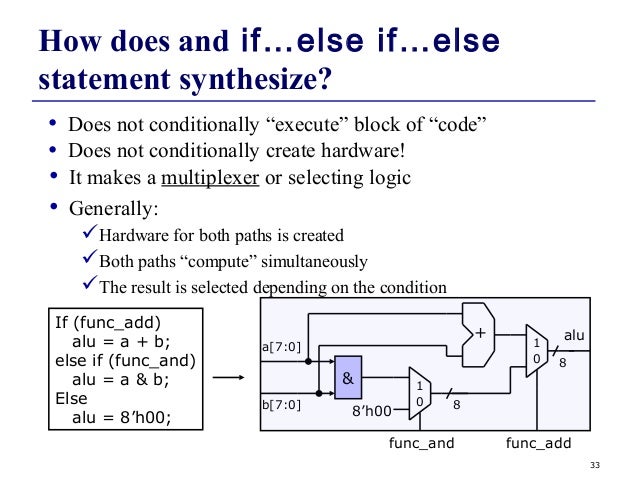
- Conditional assignments
(if/else or case statements) must be complete. No missing cases!
A wire cannot be in an undefined state and a wire has no memory!
Failure to follow this rule means inferred latches.
(from http://www.asicguru.com)
- There are no standard word sizes. You must specify the width of every wire, register, and literal.
Literals which are not specified are 32 bit, decimal constants.
For example the constant 1 defaults to 32'd1.
It is a very good idea to control width.
- Signed arithmetic has to be handled carefully. All signals default to unsigned!
Mixing signed/unsigned can have confusing consequences.
The general rule is if any operand is unsigned, the operation defaults to unsigned.
This is devastating for signed compares and signed right-shift (>>> operator)!
You may want to read signed verilog, Representation of Number Literals,
- Cyclone5 has no
automatic support for floats, but of course, you can write your own floating point.
- The value of a wire bit can be 0, 1, x (don't care), or z (high Z). Be very careful using x or z.
Here is an example of a case statement using don't care.
Only physical i/o pins on the Cyclone5 allow high impedance using tristate drivers.
- You can store variables in memory, but only if you build a memory and memory controller.
- Each signal (wire or register) may be assigned at only one location in a Verilog design,
because you cannot connect multiple voltage sources to a wire.
- That means each wire is defined in one assign statement or one always block.
- Statements within an always block which do multiple assignments, such as if/else or case statements,
actually form multiplexers.
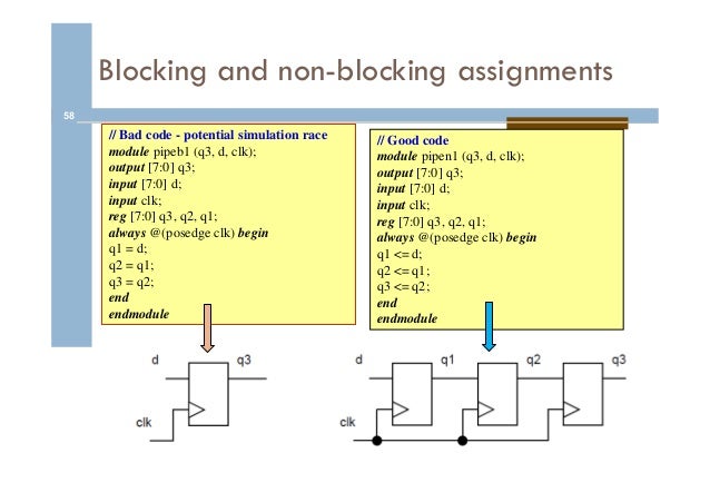
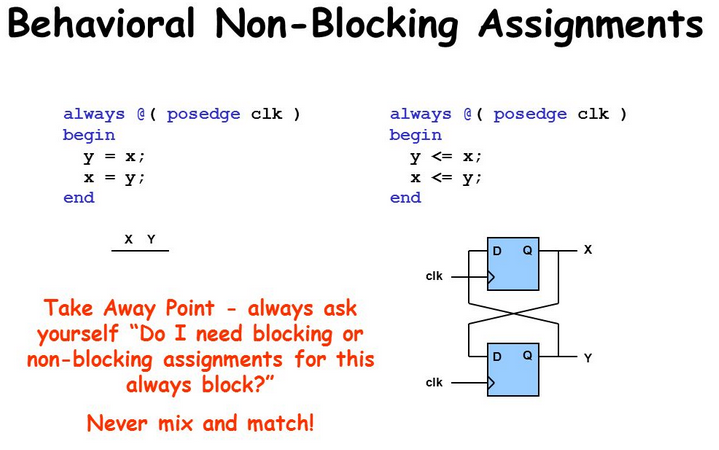
Blocking versus non-blocking assign
There are two ways to assign a value, which have different hardware consequences.
- Non-blocking assigns are indicated by the <= operator.
Use this assign in all clocked-logic always blocks to enforce simultaneous register writes on the clock edge.
- Blocking assigns are indicated by the = operator.
Use this assign in all combinatoral-logic always blocks to allow sequential statements to infer a logic structure.
But remember that there is no sequential execution within the block.
- Never mix the two forms in one block! It becomes difficult to debug.
- Example blocking results in incorrect pipeline -- be sure to look at the synthesis part at the bottom of the page.
- Example blocking results in incorrect pipeline
- Example using blocking to infer combinatorial logic
- Comparision blocking/nonblocking for swapping two signals
Pay attention to warnings and read the synthesis report
- Inferred latches -- always search warnings for inferred.
Makes timing analysis difficult or impossible and the design will probably not work.
- Implicit declaration of wires -- always search warnings for implicit.
Using the command:
`default_nettype none
will force undeclared signals to throw an error.
An implicit declaration is legal by default, but results in a 1-bit wide wire signal.
The killer is to misspell a reset signal or other control line.
wire reset;
assign reset = ~KEY[0] ;
my_cool_processor proc1(.reset(reste), ...);
- Read the synthesis report to verify actual use of DSP and memory blocks
and to make sure nothing was optimized away which should be there.
Examples
- Multiplexer (asic-world) 3 different ways
- Setting up a testbench for a computational module and getting output to compare to matlab
- Memory
- State machine (lab 1) DDA page
- Direct Digital Synthesis (DDS) of sine wave state machine and inferred ROM (full code)
 ...
// The data for the DACs
wire signed [15:0] audio_outL, audio_outR ;

// DDS sine wave generator
// for two phase-locked outputs
reg [31:0]	DDS_accum, DDS_incr;
wire signed [15:0] sine_out, sine_out_90;

// output two sine waves in quadrature
assign audio_outR = sine_out;
assign audio_outL = sine_out_90;

// DDS accumulator at audio rate
always@(posedge AUD_DACLRCK) begin
	// generate variable frequency
	// DDS F = (SW*2^14)*(audio clock rate)/(2^32)
	//
	DDS_accum = DDS_accum + {SW[17:0], 14'b0} ;
end

//hook up the ROM table for sine generation
sync_rom sineTable(CLOCK_50, DDS_accum[31:24], sine_out);
//hook up the ROM table for 90 degrees phase shift (64/256)
sync_rom sineTable_90(CLOCK_50, DDS_accum[31:24]+8'd64, sine_out_90);
endmodule

//////////////////////////////////////////////
////////////	Sin Wave ROM Table	////////////
//////////////////////////////////////////////
// produces a 2's comp, 16-bit, approximation
// of a sine wave, given an input phase (address)
module sync_rom (clock, address, sine);
input clock;
input [7:0] address;
output [15:0] sine;
reg signed [15:0] sine;
always@(posedge clock)
begin
    case(address)
    		8'h00: sine = 16'h0000 ;
			8'h01: sine = 16'h0192 ;
			8'h02: sine = 16'h0323 ;
			8'h03: sine = 16'h04b5 ;
			8'h04: sine = 16'h0645 ;
			8'h05: sine = 16'h07d5 ;
			8'h06: sine = 16'h0963 ;
			8'h07: sine = 16'h0af0 ;
			8'h08: sine = 16'h0c7c ;
			...
			8'hfb: sine = 16'hf82b ;
			8'hfc: sine = 16'hf9bb ;
			8'hfd: sine = 16'hfb4b ;
			8'hfe: sine = 16'hfcdd ;
			8'hff: sine = 16'hfe6e ;
	endcase
end
endmodule
/////////////////////////////////////////////
Copyright Cornell University
January 16, 2026