Due to the complexities involved in utilizing DMA, our original plan had to be trimmed down. Nonetheless, we were able to create two demonstrations of DMA that can be further expanded upon to create complex, high-performance graphics and animations on the PIC. First, we were able to show DMA moving a data array on the PIC32 to the SPI buffer of the TFT. Our second demo involved enabling the DMA controller to perform reads from a RAM chip. Much of the work done for this project could be considered “exploration,” as we had to dig deep into the reference manuals and create a unique system.
The TFT communicates to the PIC32 using serial peripheral interface (SPI). SPI interfaces have 4 wires, 3 of which can be shared between any number of peripherals. The 3 shared wires are clock, master out slave in (MOSI) and master in slave out (MISO). Each peripheral also has an independent chip select line from the SPI master. Most of the wires are generated by the SPI master. In the case of the PIC32’s SPI controller acting as SPI master in its default mode, the SPI clock signal will only be generated when the controller is transmitting data to one of the peripherals. Likewise, the SPI controller will only read from MISO when it is sending data over MOSI.
The Direct Memory Access (DMA) channels are complex pieces of hardware which utilize the PIC32’s internal memory bus to directly copy memory from one location to another when activated by the CPU or some interrupt, including those generated by peripherals. Due to the PIC32’s peripheral devices being memory mapped, the DMA channels can easily interact with all PIC32’s peripherals. Several DMA channels can be triggered by a single interrupt and to decide which order the DMA channels run in, the DMA controller utilizes DMA “priority.” If not modified, DMA channels with a lower id will run before DMA channels with a higher priority (DMA 0 would run before DMA 1), though for long transfers they will sometimes alternate running. If the priority of the DMA channels is modified, DMA channels with a higher DMA priority will take absolute control over the memory bus, blocking the other channels until the higher priority channel no longer needs the channel.Our design was supposed to have two RAM chips that were mapped to one of the PIC32’s SPI channels. The RAM chips would be used to store a frame buffer, which the PIC’s DMA channels would send to the TFT via the SPI channels on the PIC32. By offloading the writing of the frame buffer to the TFT, we would expect that the PIC32 could more easily keep up with the timing that would be needed to run DOOM. While the CPU is calculating the pixels for the next frame on one RAM chip, the DMA would be writing the current frame, on another RAM chip, to the TFT without needing to interact at all with the CPU.
The TFT and PIC32 are already connected together on the SECABB v2 board, with the board traces linking the B0, B2, B11 and B14 pins on the PIC32 to the TFT as well as providing independent ground and power (Appendix D.1). The TFT’s chip select line also has an exposed jumper that is normally linked to the PIC32’s B1 pin. The main communication protocol between the PIC32 and the TFT consists of a standard 4 wire SPI interface, along with power, ground and a special wire called data/command select. The special data and command select wire allows the SPI master to control how the TFT interprets the received data. For the hardware on the PIC32 side, there are 2 important hardware peripherals, the SPI controllers and the direct memory access (DMA) channels. For the hardware on the PIC32 side, there are 2 important hardware peripherals, the SPI controllers and the direct memory access (DMA) channels.
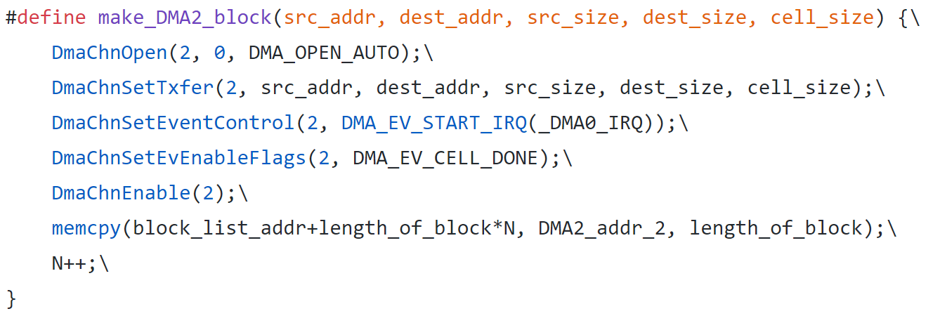
The most important feature of the DMA channels that we use in this project is the ability of a DMA channel to interface with and write data to change the behavior of another DMA channel because the DMA channel settings are mapped to a location in memory since it is a peripheral. Using this idea and previous work done by Bruce Land and Joseph Primmer (Appendix C, DMA Weird Machine), we were able to construct a rudimentary DMA processor, also called the DMA weird machine, which took instructions from memory and wrote them into the control registers for a different DMA channel which would then execute them. Each DMA instruction consists of the state of multiple different control registers for some DMA channel. We call each instruction a DMA block, as it consists of a block of control registers. The DMA block instruction contains the size of transfer, the address of the source and destination, and their respective sizes. It also contains the id of the interrupt that will cause the channel to trigger a transfer, usually the executing channel triggers when the fetching channel has completed its transfer. However, if the execution is not triggered off of the fetching channel finishing its transfer, it is important that the executing channel be placed at a lower priority, to ensure that the execution doesn’t occur before the fetching channel finishes loading the instruction.Since all the instructions in the DMA processor are exclusively move operations, it makes understanding the program extremely difficult even when compared to assembly. For example, a simple task like branching, takes at least 4 instructions, and needs a lookup table in memory to determine the result of the branch operation. The value is read into the lowest byte of address of the lookup table that holds pointers to the locations for the next instruction to execute. The pointer (next_read_addr) is then read into the address field of the instruction 2 blocks ahead of the executing block. The next block modifies the channel that is fetching the instructions so that it will now fetch from next_read_addr and continue executing the DMA program from there.
The final detail of the DMA weird machine is that the instruction cycle time is dependent on the size of the transfers completed. The DMA blocks that we utilize are 132 bytes in length because this length allows us to change the interrupt that the executing DMA channel is triggered off of, on the fly. The reason why the block size is so big is because each DMA channel has 3 shadow registers along with the default register which can set, read the inverse, and clear the selected bits. These operations are also memory mapped in between each control register which results in the DMA blocks taking up much more memory than one would initially expect.The PIC32 has 2 SPI controllers to go along with the 2 SPI channels that are available on the PIC32. The controllers also handle the data interaction between the other parts of the PIC32 and the SPI channel. The main part of the SPI channel’s data interface is the SPI Buffer. In the default mode, this buffer consists of a 32 bit register which, when written to by the CPU, will initiate an SPI transaction which will send 8, 16, or 32 bits of data from the buffer and into the data lines, depending on which mode that the SPI controller is in. The result, which is received simultaneously, is then written into the SPI buffer.
There are multiple other modes for the SPI controller but the most relevant one for this project is Framed SPI mode. In Framed SPI mode, the SPI controller takes as much control as it can away from the CPU. This means that the SPI controller will now control the chip select line automatically. It also makes the SPI clock run continuously, whereas in normal mode the SPI clock only runs when there is a transfer actively happening. This basically means that the SPI controller is set up to interact with a single peripheral. The reason why this mode is important is because this is the only mode that a DMA channel can cause the SPI controller to write to the SPI channel. In all other modes, the SPI controller doesn’t respond to the DMA channel’s write.The usage of framed mode necessitated a change in the hardware configuration that is normally used on the SECABB v2 board. The TFT_CS pins which are usually connected with a jumper were disconnected because the chip select line was now connected to the SPI controller and could only be mapped to a different output pin, which necessitated running a wire to connect the TFT_CS line to the B3 pin on the board. Pin B3 was mapped to the chip select line generated by the SPI controller (SS1) through the PIC32 peripheral pin select muxes (PPS).
The most important configuration for our usage of framed SPI mode (enabled with the SPICON_FRMEN option) on the PIC32, was the configuration of the SPI controller’s generation of chip select (CS). There are a number of options to control how the chip select is generated, the polarity of the CS (active high or low), the length of the CS and the triggering of CS relative to the first bit of data sent from the SPI controller. The TFT cannot have the CS constantly held in active low because it results in the TFT basically never updating. For the TFT, the required framed mode settings were:
Since these SPI writes are all written to the TFT buffer, we decided that we could mimic this structure using DMA. The DMA weird machine code developed by Bruce Land creates macros, or blocks, which copy the control register states for a DMA channel into a stack-allocated array which is used to create a DMA instruction (Figure 1). This standard way of creating a memory transfer block allows for us to specify where a chunk of memory is to be moved to, and how much is sent in a single transfer. In this macro, we can also specify when a block is supposed to start performing a transfer. By instantiating multiple DMA blocks with different input parameters, larger programs can be made. Using these DMA blocks, we worked to mimic the movement of data to registers in the same way as the tft_master.c code.
Unfortunately, after weeks of debugging, we were able to simulate the two commands but the commands didn’t seem to draw anything on the TFT. We were even able to execute an arbitrary series of the two commands but that didn’t translate that into the drawing actually being shown on the PIC32. In our debugging, we were able to confirm that our program structure was correct and that memory moves were happening by printing relevant variables to the TFT. Here we were essentially able to execute any function based on an array of function pointers. We also realized that this structure would not be practical because we would easily fill up the memory constraints of the PIC with the massive data structures needed to complete this design. Each extra loop through the DMA program would have required approximately 20 bytes of memory. Considering that the DMA program would likely have to be at least 200 instructions long (one for every pixel in a vertical line drawn for the TFT resolution that we would be using), we would have needed around 35% of our available RAM space just to store the data needed to execute this method.
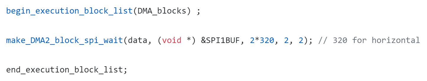
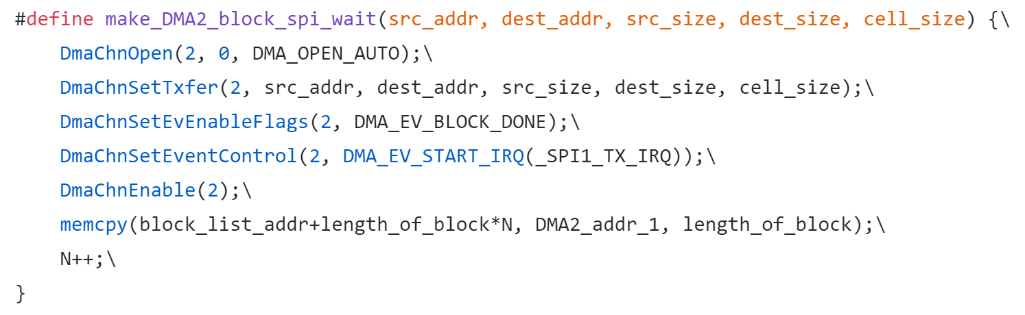
Initially, we also wanted to specify the creation of the drawing address window via DMA, however that was not able to work, as we ran into the same problems mentioned above. We initially thought that our graphics weren’t working because this function was not being done correctly in DMA. However, even when reverting the address window initialization back to its tft_master.c form, we still encountered issues. Nonetheless, to reduce the number of moving parts, we decided that we could leave the tft_setAddrWindow() call as is because this only happens once at the start of the program.Going back to the drawing board, we ended up creating a simpler structure that would directly write an array to the TFT’s SPI buffer (Figure 2) (See DMA_TFT.c in Appendix F). This approach allowed us to draw pixels to the TFT based on the contents of a 320 element data array which stores pixel colors. The one downside of this approach is that it can only draw vertical lines. Since there is no way to specify rows or columns, each element in the 320 long array represents the color for the entire column. The make_DMA2_block_spi_wait() DMA block is created with the same macro as in the DMA weird machine (Figure 3). Here, we specify the block transfer to begin on the _SPI1_TX_IRQ. This IRQ signifies the completion of an SPI transfer. In our code, whenever all 320 elements in the data array are written to, the DMA block will initiate the transfer of this data into the TFT’s SPI buffer, which will result in colors being drawn on the screen. With the DMA channel active, the TFT would be updated every time the 320 element data array was defined.
However, this solution introduced another problem. Since the SPI clock (SCLKx) is always being sent by the SPI controller when the SPI channel is running in framed mode, the RAM chip would constantly be receiving clock signal while the chip select was held low and so the RAM chip would interpret the inactive MOSI line as data being sent from the PIC32, since the clock was running and CS is held low. Both the PIC32 and our DMA processor are not fast enough to lower CS and immediately start a data transfer in the same SPI clock cycle. This means that the RAM would incorrectly read the data sent on the SPI channel from the PIC32 as shifted by a large number of bytes which means that the read command would fail and the RAM wouldn’t send the expected response. The only solution with that SPI setup would be to decrease the SPI clock frequency to be slow enough that the DMA processor can trigger a transfer before the next clock cycle, which would lose much of the speed benefits that the frame buffer gains.
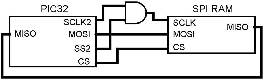
The solution that we thought of to use the RAM in framed mode was to make framed mode behave like the PIC32’s default SPI mode. We had already progressed in this direction by not using SS2 and using a GPIO generated CS. The only change we would need to make to the framed SPI mode signal behave like the default SPI mode would be to have the SPI clock only run when there is a transfer occurring. Since SS2 can be configured to be active high only when there is a transfer occurring, using a logical AND gate between the SCLK line and the SS2 would result in the RAM chip receiving an SPI signal as if the PIC32’s SPI channel was in its default mode of operation. The diagram D.2 in Appendix D, shows the configuration of the signals sent between the PIC32 and RAM.
The configuration of the SPI mode for this setup was slightly different from those used to interact with the TFT because SS2 needed to be active high to let the SCLK control the signal when there was a transfer occurring. The SPI configuration settings were:This configuration let the provided SPI RAM software function in framed SPI mode, though there were still some bugs. The main bug was that when we read from the RAM chip, the PIC32 returned a value one half the value that we expected. This seemed to indicate that the PIC32 was reading an extra bit before the RAM was sending data. Because the PIC32’s SPI controller can only send and receive data in byte length packets, we eventually determined that the SPI RAM was sending data much later than the PIC32 was reading the data. We could confirm that this was the case because when we decreased the SPI clock speed from 20MHz to 2 MHz we found that this bug disappeared and that the RAM chip functioned exactly as expected.
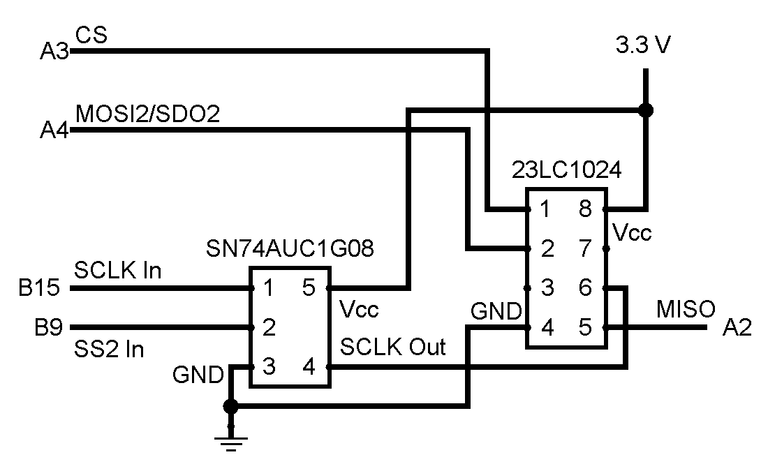
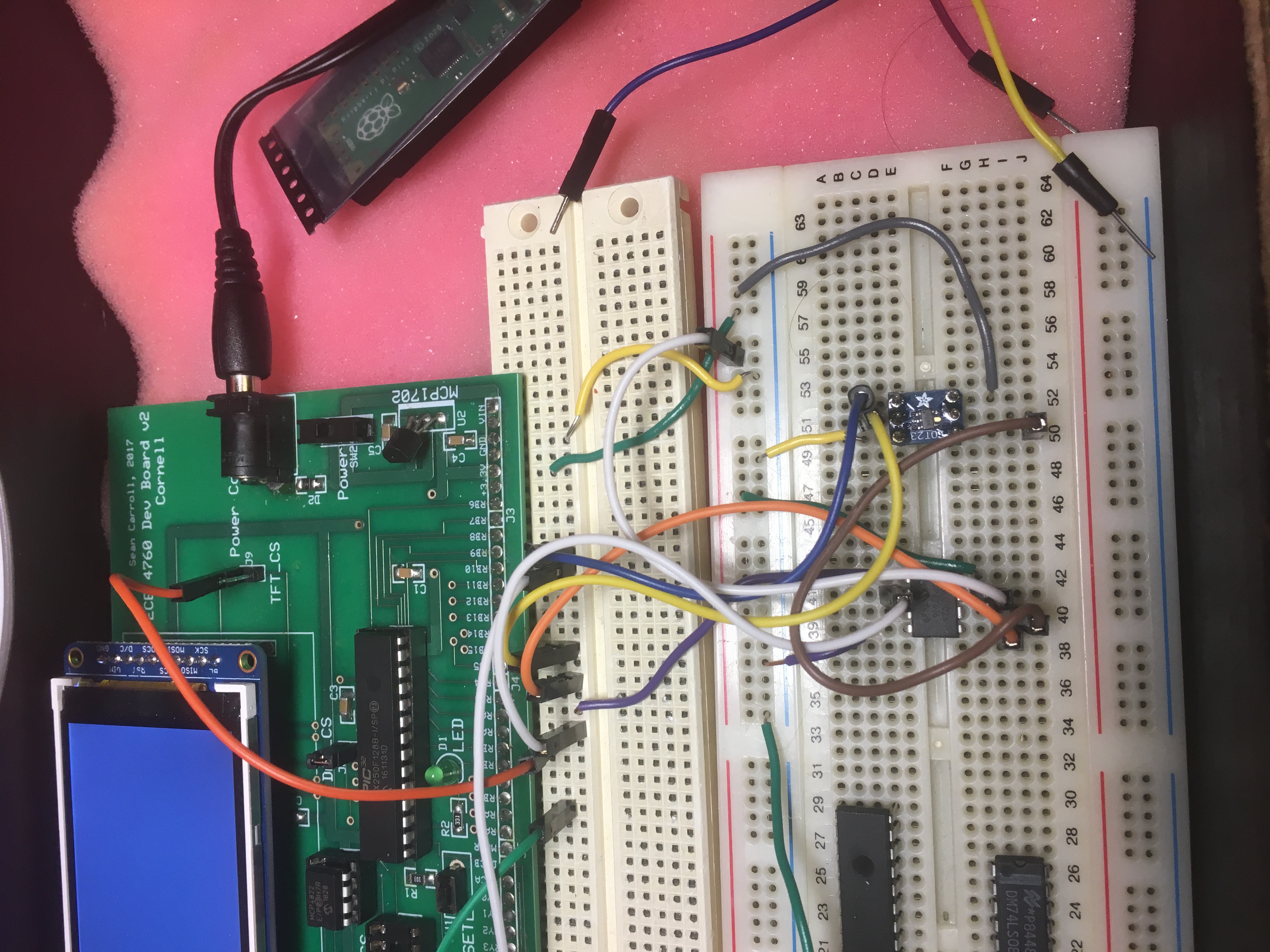
Further investigation with an oscilloscope led to the conclusion that the SPI RAM’s SCLK was delayed by about 30% of the clock period with the SCLK sent by the PIC32 when running at 20 MHz. The reason for this was that our initial logical AND gate was the DM74LS08 had a propagation delay which was a significant fraction of the SCLK cycle time. The SCLK was running at 20MHz, which meant that it had a period of 50 ns, with a 50% duty cycle square wave. The AND gate had a proportional delay of about 13-18 ns which meant that the RAM was receiving the clock approximately half a cycle after the PIC32 sent it. This was barely enough to let the SPI RAM receive commands but meant that the PIC32 sampled the MISO line before the RAM could set up the clock line.The solution to this problem was to purchase a significantly faster AND gate which had a setup time that was much fatter than the cycle time. The product that we purchased was the SN74AUC1G08, a high frequency AND gate which had a propagation delay of at most 2 ns, less than a 20th of the clock cycle. Substituting the new AND gate for the DM74LS08 and running at 20 MHz clock rate resulted in the expected behavior of the SPI chip. The physical implementation of the RAM and AND gate circuit is shown in Appendix D.4
The DMA structure we devised starts with a DMA channel sending the read address to the RAM chip, and reading the junk response. After this, we use three DMA channels to complete the read. One channel writes junk to the SPI2BUF to force the SPI channel to read incoming data from MISO as well as generate clock signals to send to the RAM. Another channel reads the data from the SPI2BUF of the RAM chip into the output array. The last channel is used to clear the interrupt from the channel that is reading from the transfer buffer, so that the channel that writes junk can be triggered multiple times. Once completed, we needed to disable the three DMA channels we used because one channel is used for printing to UART, and the other two channels we do not want to get accidentally triggered outside the DMA read function. This action allowed us to preserve the DMA state while running the DMA program. When defining the operations of these DMA channels, we needed to take extra precautions regarding UART and SPI communication. Specifically, we added NOPs before initiating the actual reading so that the CPU wouldn’t print a response to the UART terminal before the response was read from SPI.
Here is a link to our demo, showing the results of our project: Demo
The final output of our project was two demonstrations of DMA used on the PIC32. The first demo showed the TFT being drawn via DMA data transfers to the TFT’s SPI buffer. To visualize this, we created a sequence which updated the 320 element array with different colors. A video of this can be seen below in Figure 5.
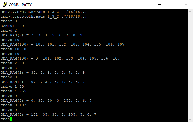
The second demo had DMA channels set up to read from a RAM chip. A sample terminal output can be seen below. The ‘w’ command is the write byte command, the ‘r’ command is the read byte command, the ‘d’ command reads a series of bytes through DMA.. Upon initialization we set the value of each memory address to itself modulo 256 so that we have expected values.
With consideration of intellectual property, we need to consider that we used code which was designed by others. The first of these is the DMA Weird Machine, created by Bruce Land. The second of these is the UART SPI RAM code, also made by Bruce Land. The last of these is the TFT draw code, originally written by Limor Fried and subsequently rewritten by Syed Tahmid Mahbub. In our original plans to port DOOM, we would have used the open-source code that is available on GitHub. Since we did not end up porting DOOM, we did not use that code base. However, we still included it in our Appendix C for interest’s sake. Despite using much open-source code, we do not use code in the public domain. We don’t really see many patent opportunities for the project, and there does not seem to be many opportunities for publishing either. However, this project provides a great infrastructure for someone to develop complex, high performance graphics with. If someone were to expand upon this project, patent/publishing opportunities may arise. Nonetheless, for someone who wants to really dive deep into DMA and SPI on a PIC32, this project could be of great interest and use.
We don’t really see any ethical considerations here. There is nothing done in this project that could put anyone in serious and immediate danger if something went wrong. Diving deep into DMA is unlikely to lead to any future technologies that would be of ethical concern, either.Besides typical lab safety, there are really no safety concerns. Most of our project was based on hardware interaction inside the PIC32 and the external hardware we did was simple breadboard wiring, which had a maximum voltage of 3.3 V and maximum current around 10 mA.
In terms of any legal considerations, we really only have to worry about using other people’s open-source code. Because of this, we would have to consider the implications of that before doing anything with our own code.Overall,this project was a great experience for us and we most certainly got a lot of experience working with low-level programming and hardware interaction on the PIC32.
"The group approves this report for inclusion on the course website."
"The group approves the video for inclusion on the course youtube channel."
| Part | Price | SECABB v2 | $10 |
| PIC32MX250F128B | $5 |
| ILI9340 TFT LCD | $10 |
| 23LC1024 RAM Chip | $2.50 |
| SOT23 Carrier | $1 |
| SN74AUC1G08 AND Gate (Mouser) | $0.50 |
| Wires | $1.50 |
| Total | $30.50 |
For references, here are the resources we used. We included standard links as well as links to the Wayback Machine, when possible, for posterity’s sake.
The following are links to datasheets for the components we used.
23LC1024:
Datasheet, Wayback MachineDM74LS08:
Datasheet, Wayback MachineSN74AUC1G08:
Datasheet, Wayback MachineILI9340:
Datasheet, Wayback MachineNow, here are links to any software we used, or, in the case of DOOM, would have used.
Bruce Land's DMA Weird Machine
Code, Wayback MachineBruce Land’s UART SPI RAM code:
Code, Wayback MachineSPI Information, Wayback Machine
Syed Tahmid Mahbub’s Blog page on TFT and PIC32, as well as a Google Drive link to the TFT files:
Blog Page, Wayback Machine, Google Drive LinkDOOM GitHub code (not actually used):
Github, Wayback MachineAnd, lastly, any other resources we used.
Sean Carroll’s Dev Board Schematic:
Schematic, Wayback MachineCode highlighter
Prism.js
Much of the work that was done for this lab was done together in the lab throughout the week and especially during our lab hours.
/*
 * File:        DMA TFT Graphics
 * Author:      Christopher Bakhos, Tyrone Whitmore-Wilson, Stephen Zakoworotny
 * Target PIC:  PIC32MX250F128B
 */

////////////////////////////////////
// clock AND protoThreads configure!
// You MUST check this file!
#include "config_1_3_2.h"
// threading library
#include "pt_cornell_1_3_2_python.h"

////////////////////////////////////
// graphics libraries
#include "tft_master.h"
#include "tft_gfx.h"
// need for rand function
#include <stdlib.h>
// fixed point types
#include <stdfix.h>
#include <math.h>
////////////////////////////////////


/* Demo code for interfacing TFT (ILI9340 controller) to PIC32
 * The library has been modified from a similar Adafruit library
 */
// Adafruit data:
/***************************************************
  This is an example sketch for the Adafruit 2.2" SPI display.
  This library works with the Adafruit 2.2" TFT Breakout w/SD card
  ----> http://www.adafruit.com/products/1480

  Check out the links above for our tutorials and wiring diagrams
  These displays use SPI to communicate, 4 or 5 pins are required to
  interface (RST is optional)
  Adafruit invests time and resources providing this open source code,
  please support Adafruit and open-source hardware by purchasing
  products from Adafruit!

  Written by Limor Fried/Ladyada for Adafruit Industries.
  MIT license, all text above must be included in any redistribution
 ****************************************************/

// ==============
// Block list macros to make defining a list of blocks easier
//
// Register offsets into the DMA control block
// BUT since we are starting the DMA block transfer on the SSA field
//#define DCH0ECON_OFFSET 0x10 // first variable field
#define DCH0SSA_OFFSET  0x30 // DMA source address field
#define DCH0SSIZ_OFFSET 0x50-DCH0SSA_OFFSET // DMA source size
#define DCH0CSIZ_OFFSET 0x90-DCH0SSA_OFFSET // DMA cell size

// the source address required for the next block to be defined
// N is a counter incremented by the block definition macros below
#define next_blk_src_addr (void*)(DMA_blocks+length_of_block*(N+1))
#define second_blk_src_addr (void*)(DMA_blocks+length_of_block*(N+2))

// the address of the next block to be defined
#define next_blk_addr (void*)(DMA_blocks+length_of_block*(N+1))

// the hardware address of DMA0 control block
#define DMA0_addr (void*)&DCH0CON
#define DMA0_addr_1 (void*)&DCH0ECON
// The address of DMA0 second word
#define DMA0_addr_2 (void*)&DCH0SSA

// the hardware address of DMA2 control block
#define DMA2_addr (void*)&DCH2CON
#define DMA2_addr_1 (void*)&DCH2ECON
// the hardware address of DMA2 second word
#define DMA2_addr_2 (void*)&DCH2SSA

// use a SFR in a DMA block as a scratch register for doing bit arithmetic
// operations using the set/clr/inv registers associated with each SFR
// A MOV to the set/clr/inv registers performs the bit-wise operation
// "transport triggered operations"
//  -- OR -- write a variable into the register, then write another variable to SET, read result
//  -- NOT -- write a variable into the register, then write 0xff to INV, read result
//  -- AND -- invert both variables, OR them, invert result
#define scratch_sfr (void*) &DCH3DAT// terminate match byte
#define scratch_sfr_set (void*)&DCH3DATSET
#define scratch_sfr_clr (void*)&DCH3DATCLR
#define scratch_sfr_inv (void*)&DCH3DATINV
// and another set
#define scratch_sfr_2 (void*) &DCH1DAT// terminate match byte
#define scratch_sfr_set_2 (void*)&DCH1DATSET
#define scratch_sfr_clr_2 (void*)&DCH1DATCLR
#define scratch_sfr_inv_2 (void*)&DCH1DATINV

// ==============
// macros to begin and end execution block list
#define begin_execution_block_list(list_name) {\
    N=0;\
    block_list_addr = list_name;\
}

//number_of_blocks = N;
#define end_execution_block_list {\
}


// ==============
// A macro to make defining DMA2 blocks more terse
// DMA2 blocks are the op-codes of the DMA machine
// Uses PLIB DMA macros to build a block, then copy it to the block-list array
// which is the DMA program
//


#define make_DMA2_block(src_addr, dest_addr, src_size, dest_size, cell_size) {\
    DmaChnOpen(2, 0, DMA_OPEN_AUTO);\
    DmaChnSetTxfer(2, src_addr, dest_addr, src_size, dest_size, cell_size);\
    DmaChnSetEvEnableFlags(2, DMA_EV_CELL_DONE);\
    DmaChnSetEventControl(2, DMA_EV_START_IRQ(_DMA0_IRQ));\
    DmaChnEnable(2);\
    memcpy(block_list_addr+length_of_block*N, DMA2_addr_1, length_of_block);\
    N++;\
}

#define make_DMA2_block_spi_wait(src_addr, dest_addr, src_size, dest_size, cell_size) {\
    DmaChnOpen(2, 0, DMA_OPEN_AUTO);\
    DmaChnSetTxfer(2, src_addr, dest_addr, src_size, dest_size, cell_size);\
    DmaChnSetEvEnableFlags(2, DMA_EV_BLOCK_DONE);\
    DmaChnSetEventControl(2, DMA_EV_START_IRQ(_SPI1_TX_IRQ));\
    DmaChnEnable(2);\
    memcpy(block_list_addr+length_of_block*N, DMA2_addr_1, length_of_block);\
    N++;\
}

// ==============
// A macro to make defining DMA0 blocks more terse
// DMA0 blocks are efffectively the program counter for the DMA machine
//    DmaChnSetEventControl(0, DMA_EV_START_IRQ(_TIMER_2_IRQ));\
//

#define make_DMA0_block(src_addr, dest_addr, src_size, dest_size, cell_size) {\
    DmaChnOpen(0, 0, DMA_OPEN_AUTO);\
    DmaChnSetTxfer(0, src_addr, dest_addr, src_size, dest_size, cell_size);\
    DmaChnSetEvEnableFlags(0, DMA_EV_CELL_DONE);\
    DmaChnSetEventControl(0, DMA_EV_START_IRQ(_DMA2_IRQ));\
    DmaChnEnable(0);\
    memcpy(block_list_addr+length_of_block*N, DMA0_addr_1, length_of_block);\
    N++;\
}

// ==============
// Sequence labels
// These will be given values in the block-list definition stage to identify jump-targets
int DMA_begin_label;
// A macro to assign a sequence label value
// just copies the next block count to a label variable
#define branch_label() N
#define branch_label_to_addr(label) ( DMA_blocks + (label)*length_of_block )


//DMA data
// volatile unsigned int* program[9] __attribute__ ((aligned(256))); //Sequence of DMA labels
volatile unsigned short data[1000]; //Sequence of tft data

//Consts for DMA pixel draw
// const char dc_cs = 0b11; // used for toggling dc and cs
const char dc = 0b01; // used for just toggling dc
// const char cs = 0b10; // Used for just toggling cs
const short Mode = 0x400;


// volatile unsigned char data_counter = 0; // Incremented by 1, used to index into data_offset_array
// volatile unsigned char command_counter = 0; // Incremented by 1, used to index into command_offset_array
// volatile unsigned char program_counter = 0; // Incremented by 1, used to index into program_offset_array
// unsigned char program_offset_array[] __attribute__ ((aligned(256))) = {0, 4, 8, 12, 16, 20, 24, 28, 32} ;
// unsigned char data_offset_array[] __attribute__ ((aligned(256))) = {0, 2, 4, 6, 8, 10};
unsigned char inc_arr[240] __attribute__ ((aligned(256)));


volatile unsigned short bit_bucket;
// volatile unsigned int** addr = program;
volatile unsigned int* next_program_addr;
//Sequence Labels
volatile int spi_write16_label = 0;
volatile int DMA_wait_label = 0;
volatile char column_set = ILI9340_CASET;
volatile char row_set = ILI9340_PASET;
volatile char ram_write = ILI9340_RAMWR;
unsigned short clear_flag = 0x0000;
unsigned short T2clear_flag = 0x00000200;
unsigned short size;


// ==============
// DMA block image list
// The machine will cycle through these blocks, then start again
// But branching may shift execution to a different list

// From http://people.ece.cornell.edu/land/courses/ece4760/PIC32/Microchip_stuff/2xx_datasheet.pdf
// page 52, TABLE 4-12:DMA CHANNELS 0-3 REGISTER MAP
// Total DMA control block size in bytes:
#define length_of_block 132
// the main DMA block program list
// max of 50 blocks!
#define max_blocks 2
unsigned char DMA_blocks[max_blocks * length_of_block];
// base address of DMA block list being defined
unsigned int block_list_addr ;
// counter for the current block to create
int N = 0;

// string buffer
char buffer[60];

// === thread structures ============================================
// thread control structs
// note that UART input and output are threads
static struct pt pt_timer ;


static PT_THREAD (protothread_timer(struct pt *pt))
{
  PT_BEGIN(pt);
    while(1) {
      // yield time 1 second
      sys_time_seconds++ ;
      // toggle the LED on the big board
      // draw sys_time
      sprintf(buffer,"%d, %X", sys_time_seconds, bit_bucket);
      printLine(0, buffer, ILI9340_YELLOW, ILI9340_BLACK);
      sprintf(buffer, "%X, %X", DCH2SSA, DCH2DSA);
      printLine(1, buffer, ILI9340_YELLOW, ILI9340_BLACK);
      sprintf(buffer, "%X, %X", DCH0SSA, DCH0DSA);
      printLine(2, buffer, ILI9340_YELLOW, ILI9340_BLACK);
      sprintf(buffer,"DMA2 src:%X, DMA2 dest:%X,", &DCH2SSA, &DCH2DSA);
      printLine(7, buffer, ILI9340_YELLOW, ILI9340_BLACK);
      sprintf(buffer, "DMA0 src:%X, DMA0 dest:%X,", &DCH0SSA, &DCH0DSA);
      printLine(8, buffer, ILI9340_YELLOW, ILI9340_BLACK);
      sprintf(buffer,"data_arr addr:%X", (short) data);
      printLine(9, buffer, ILI9340_YELLOW, ILI9340_BLACK);
      // sprintf(buffer,"data_inc addr:%X, inc addr:%X, prog_inc addr:%X",(short)  data_offset_array, (short) inc_arr, (short) program_offset_array);
      // printLine(10, buffer, ILI9340_YELLOW, ILI9340_BLACK);
      sprintf(buffer,"block_arry start addr:%X  block_arry end addr:%X",(short) DMA_blocks, (short) &DMA_blocks[(max_blocks*length_of_block)-1]);
      printLine(11, buffer, ILI9340_YELLOW, ILI9340_BLACK);


      PT_YIELD_TIME_msec(1000) ;
      // !!!! NEVER exit while !!!!
    } // END WHILE(1)
  PT_END(pt);
}

// printLine function to print info to the TFT :)
void printLine(int line_number, char* print_buffer, short text_color, short back_color){
    // line number 0 to 31
    /// !!! assumes tft_setRotation(0);
    // print_buffer is the string to print
    int v_pos;
    v_pos = line_number * 10 ;
    // erase the pixels
    tft_fillRoundRect(0, v_pos, 239, 8, 1, back_color);// x,y,w,h,radius,color
    tft_setTextColor(text_color);
    tft_setCursor(0, v_pos);
    tft_setTextSize(1);
    tft_writeString(print_buffer);
}
// === Main  ======================================================
void main(void) {
 //SYSTEMConfigPerformance(PBCLK);

  ANSELA = 0; ANSELB = 0;

  // === config threads ==========
  // turns OFF UART support and debugger pin, unless defines are set
  PT_setup();

  // === setup system wide interrupts  ========
  INTEnableSystemMultiVectoredInt();

  // init the display
  tft_init_hw();
  tft_begin();
  tft_fillScreen(ILI9340_BLACK);
  //240x320 vertical display
  tft_setRotation(1); // Use tft_setRotation(1) for 320x240

  begin_execution_block_list(DMA_blocks) ;

  make_DMA2_block_spi_wait(data, (void *) &SPI1BUF, 2*320, 2, 2); // 320 for horizontal

  end_execution_block_list;

  //data[0] = 10; // x
  //data[1] = 10; // x + 1
  //data[2] = 10; // y
  //data[3] = 239; // y + 1
  int i = 0;
  for(i = 0; i < 320/3; i++){
    data[i] = ILI9340_RED;
  }
  for(i = 320/3; i < (320*2)/3; i++){
    data[i] = ILI9340_GREEN;
  }
  for(i = (320*2)/3; i < 320; i++){
    data[i] = ILI9340_BLUE;
  }
  for(i = 0; i < 239; i++){
    inc_arr[i] = i + 1;
  }
  inc_arr[239] = 239;

  // === DMA fetch/execute setup  =====================
  // This is a general setup, without specific function until the execution block
  // list defined above is traversed, one block at a time, by DMA0 acting as a
  // fetch-from-memory to DMA2. DMA2 then produces a series of programmed moves.
  // The system is clockless, but strictly sequential because DMA0 completion triggers
  // DMA2. DMA2 completion triggers DMA0 to load the next block to DMA2.
  // !!!!!
  // This part of the code defines a state machine that does NOT need to be
  // modified for a specific DMA program
  // ==================================================
  // Open the all the  DMA channels,
  // except DMA2 which will be loaded and triggered by DMA0
  // Enable the AUTO option for all
  DmaChnOpen(0, 0, DMA_OPEN_AUTO);
  DmaChnOpen(1, 0, DMA_OPEN_AUTO);
  DmaChnOpen(2, 0, DMA_OPEN_AUTO); //-- defined on the fly from the block lists above
  DmaChnOpen(3, 0, DMA_OPEN_AUTO);

  // set the transfer parameters: source & destination address,
  //   source & destination size, number of bytes per event
  // DMA0 writes DMA control blocks from an array (DMA program) to DMA2
  // DMA1 writes to the DMA0 control block to clear a flag
  // DMA2 moves data as specified in the block array defined earlier
  // DMA3 writes to the DMA2 control block to clear a flag
  // number_of_blocks is the number defined in the execution path.
  DmaChnSetTxfer(0, DMA_blocks, DMA2_addr_1, max_blocks*length_of_block, length_of_block, length_of_block);
  //DmaChnSetTxfer(1, &clear_flag, (void*)&DCH0INT, 2, 2, 2);
  //DmaChnSetTxfer(2, LED_pattern1, (void*)&LATB, 16, 1, 1);
  //DmaChnSetTxfer(3, &clear_flag, (void*)&DCH2INT, 2, 2, 2);

  // set the transfer event control: what event is to start the DMA transfers
  // In this case, DMA0 triggers DMA2 and vice-versa
  // and cell transfer done on DMA0 triggers channel 1 to clear the DMA0 flag
  // and cell transfer done on DMA2 triggers channel 3 to clear the DMA2 flag
  // net result is to bounce between DMA0 and DMA2 as fast as possible
  // BUT you need to force a transfer to start the system
  DmaChnSetEventControl(0, DMA_EV_START_IRQ(_DMA2_IRQ)); //_TIMER_2_IRQ
  DmaChnSetEventControl(1, DMA_EV_START_IRQ(_DMA0_IRQ));
  DmaChnSetEventControl(2, DMA_EV_START_IRQ(_DMA0_IRQ));
  DmaChnSetEventControl(3, DMA_EV_START_IRQ(_DMA2_IRQ));

  // Set up the cell transfer done flags
  // needed to set up cell done enable bit
  DmaChnSetEvEnableFlags(0, DMA_EV_CELL_DONE);
  DmaChnSetEvEnableFlags(2, DMA_EV_BLOCK_DONE);

  // start the channels
  DmaChnEnable(0);
  DmaChnEnable(1);
  DmaChnEnable(2);
  DmaChnEnable(3);


  tft_setAddrWindow(0, 0, 320, 240); // Set the address widnow to the whole screen
  int j = 313;
  while(j--){
    tft_writedata16(ILI9340_CYAN);
  }
  Mode16();
  _dc_high();
  DmaChnForceTxfer(0);
  delay_us(30);
  DmaChnAbortTxfer(0);
  delay_ms(2000);
  // Demo Sequence
  i = 2;
  while(i--){
    for(j = 0; j < 320; j++){
      data[j] = ILI9340_BLUE;
    }
    delay_ms(1500);
    for(j = 0; j < 320; j++){
      data[j] = ILI9340_RED;
    }
    delay_ms(1500);
    for(j = 0; j < 320; j++){
      data[j] = ILI9340_GREEN;
    }
    delay_ms(1500);
    for(j = 0; j < 320; j++){
      data[j] = ILI9340_BLACK;
    }
    delay_ms(1500);
    for(j = 0; j < 320/3; j++){
    data[j] = ILI9340_RED;
    }
    for(j = 320/3; j < 320; j++){
      data[j] = ILI9340_BLACK;
    }
    delay_ms(1500);
    for(j = 0; j < 320/3; j++){
      data[j] = ILI9340_RED;
    }
    for(j = 320/3; j < (320*2)/3; j++){
      data[j] = ILI9340_GREEN;
    }
    for(j = (320*2)/3; j < 320; j++){
      data[j] = ILI9340_BLACK;
    }
    delay_ms(1500);
    for(j = 0; j < 320/3; j++){
      data[j] = ILI9340_RED;
    }
    for(j = 320/3; j < (320*2)/3; j++){
      data[j] = ILI9340_GREEN;
    }
    for(j = (320*2)/3; j < 320; j++){
      data[j] = ILI9340_BLUE;
    }
    delay_ms(1500);
  }
  for(i = 0; i < 320/3; i++){
    data[i] = ILI9340_RED;
  }
  for(i = 320/3; i < (320*2)/3; i++){
    data[i] = ILI9340_GREEN;
  }
  for(i = (320*2)/3; i < 320; i++){
    data[i] = ILI9340_BLUE;
  }

  // pt_add(protothread_timer, 0);

  // === initalize the scheduler ====================
  PT_INIT(&pt_sched) ;
  // >>> CHOOSE the scheduler method: <<<
  // (1)
  // SCHED_ROUND_ROBIN just cycles thru all defined threads
  //pt_sched_method = SCHED_ROUND_ROBIN ;

  // NOTE the controller must run in SCHED_ROUND_ROBIN mode
  // ALSO note that the scheduler is modified to cpy a char
  // from uart1 to uart2 for the controller

  pt_sched_method = SCHED_ROUND_ROBIN ;

  // === scheduler thread =======================
  // scheduler never exits
  PT_SCHEDULE(protothread_sched(&pt_sched));
  // round-robin scheduler for threads


  // init the threads

  // PT_INIT(&pt_timer);
  // // Initalize the scheduler - From SECABB
  // PT_INIT(&pt_sched) ;

  // // From SECABB
  // pt_sched_method = SCHED_ROUND_ROBIN ;
  //   while (1){
  //     PT_SCHEDULE(protothread_anim(&pt_anim));
  //     PT_SCHEDULE(protothread_timer(&pt_timer));
  //     // Scheduler - From SECABB
  //     PT_SCHEDULE(protothread_sched(&pt_sched));
  // }
} // main
/*********************************************************************
 * File:        DMA SPI RAM
 * Author:      Christopher Bakhos, Tyrone Whitmore-Wilson, Stephen Zakoworotny
 * Target PIC:  PIC32MX250F128B
 *
 * SPI to  23LC1024 serial RAM & DAC
 * Uses DMA channels to perform read operations on the SPI RAM
 *
 *********************************************************************
 * Based on Uart_spi_RAM_DAC.c
 * Bruce Land -- Cornell University
 * Dec 2015
 *~~~~~~~~~~~~~~~~~~~~~~~~~~~~~~~~~~~~~~~~~~~~~~~~~~~~~~~~~~~~~~~~~~~~
*/

//=== clock AND protoThreads configure =============================
#include "config_1_3_2.h"
// threading library
#include "pt_cornell_1_3_2_python.h"
//#include "spi_legacy.h"

// === thread structures ============================================
// semaphores for controlling two threads
// for guarding the UART and for allowing stread blink control
static struct pt_sem control_t1, control_t2, control_t6  ;
// thread control structs
// note that UART input and output are threads
static struct pt pt_cmd, pt_tick;
// uart control threads
static struct pt pt_input, pt_output, pt_DMA_output ;
// system 1 second interval tick
int sys_time_seconds ;

// === RAM test data ====================================================
// some data to write
unsigned char test_data[]={2, 4, 6, 8, 10, 100, 200, 255}; // 8
unsigned char test_data2[8];
unsigned char test_data3[640];

// === SPI setup ========================================================
volatile SpiChannel spiChn = SPI_CHANNEL2 ;	// the SPI channel to use
volatile int spiClkDiv = 2 ; // 20 MHz max speed for this RAM
//volatile int spiClkDiv = 4 ;

// === RAM commands ======================================================
// from 23LC1024 datasheet
// http://ww1.microchip.com/downloads/en/DeviceDoc/20005142C.pdf
// Default setup includes data streaming from current address
// This is used in the array read/write functions
#define RAM_WRITE_CMD (0x2000000) // top 8 bits -- 24 bits for address
#define RAM_READ_CMD  (0x3000000) // top 8 bits -- 24 bits for address
// command format consists of a read or write command ORed with a 24-bit
// address, even though the actual address is never more than 17 bits
// general procedure will be:
// Drop chip-select line
// Do a 32-bit SPI transfer with command ORed with address
// switch to 8-bit SPI mode
// Send one or more data bytes
// Raise chip-select line
//
// At 20 MHz SPI bus rate:
// Command ORed with address, plus mode change, takes 2.2 microsec
// Each byte takes 0.75 microseconds

/* ====== MCP4822 control word =========================================
bit 15 A/B: DACA or DACB Selection bit
1 = Write to DACB
0 = Write to DACA
bit 14 ? Don?t Care
bit 13 GA: Output Gain Selection bit
1 = 1x (VOUT = VREF * D/4096)
0 = 2x (VOUT = 2 * VREF * D/4096), where internal VREF = 2.048V.
bit 12 SHDN: Output Shutdown Control bit
1 = Active mode operation. VOUT is available. ?
0 = Shutdown the selected DAC channel. Analog output is not available at the channel that was shut down.
VOUT pin is connected to 500 k???typical)?
bit 11-0 D11:D0: DAC Input Data bits. Bit x is ignored.
*/
// A-channel, 1x, active
#define DAC_config_chan_A 0b0011000000000000
#define RAM_CS_low  {LATACLR = 0b1000;}
#define RAM_CS_high {LATASET = 0b1000;}

// === spi bit widths ====================================================
// hit the SPI control register directly
inline void RAM_Mode16(void){  // configure SPI1 for 16-bit mode
    SPI2CONSET = 0x400;
    SPI2CONCLR = 0x800;
}
// ========
inline void RAM_Mode8(void){  // configure SPI1 for 8-bit mode
    SPI2CONCLR = 0x400;
    SPI2CONCLR = 0x800;
}
// ========
inline void RAM_Mode32(void){  // configure SPI1 for 8-bit mode
    SPI2CONCLR = 0x400;
    SPI2CONSET = 0x800;
}
// === DAC byte write =====================================================
// address between 0 and 2^17-1
// data bytes
void dac_write_byte(int data){
    int junk;
    // Channel config ORed with data
    RAM_Mode16();
    mPORTBClearBits(BIT_1);
    // write to spi2 and convert 8 bits to 12 bits
    WriteSPI2(DAC_config_chan_A | (data));
    // test for done
    while (SPI2STATbits.SPIBUSY); // wait for end of transaction
    junk = ReadSPI2(); // must always read, even if nothing useful is returned
    // set 8-bit transfer for each byte
    mPORTBSetBits(BIT_1);
    return ;
}

// === RAM byte write =====================================================
// address between 0 and 2^17-1
// data bytes
void ram_write_byte(int addr, unsigned char data){
    int junk;
    // set 32-bit transfer for read/write command ORed with
    // actual address
    RAM_Mode32();
    RAM_CS_low
    WriteSPI2(RAM_WRITE_CMD | addr); // addr not greater than 17 bits
    while (SPI2STATbits.SPIBUSY); // wait for it to end of transaction
    junk = ReadSPI2(); // must always read, even if nothing useful is returned
    // set 8-bit transfer for each byte
    RAM_Mode8();
    WriteSPI2(data); // data write
    while (SPI2STATbits.SPIBUSY); // wait for it to end of transaction
    junk = ReadSPI2();
    RAM_CS_high
    return ;
}

// === RAM array write =====================================================
// address, pointer to an array containing the data, number of BYTES to store
void ram_write_byte_array(int addr, char* data, int count){
    int junk, i;
    RAM_Mode32();
    RAM_CS_low
    WriteSPI2(RAM_WRITE_CMD | addr); // addr not greater than 17 bits
    while (SPI2STATbits.SPIBUSY); // wait for it to end of transaction
    junk = ReadSPI2();
    RAM_Mode8();
    for(i=0; i<count; i++){
        WriteSPI2(data[i]); // data write
        while (SPI2STATbits.SPIBUSY); // wait for it to end of transaction
        junk = ReadSPI2();
    }
    RAM_CS_high
    return ;
}

// === RAM byte read ======================================================
int ram_read_byte(int addr){
    int junk, data;

    //Default config
    RAM_Mode32();
    RAM_CS_low
    WriteSPI2(RAM_READ_CMD | addr);
    while (SPI2STATbits.SPIBUSY); // wait for it to end of transaction
    junk = ReadSPI2();
    RAM_Mode8();
    WriteSPI2(junk); // force the read
    while (SPI2STATbits.SPIBUSY); // wait for it to end of transaction
    data = ReadSPI2();
    RAM_CS_high

    return data;
}

int ram_read_byte_dma(int addr){
    unsigned char DMA_block[192];
    memcpy(DMA_block, &DCH1CON, 192); //Store DMA channel 1 state
    int junk;
    //DMA config
    int send = RAM_READ_CMD | addr;
    int clear_flag = 0x04; //Clears cell transfer complete
    //Open DMA channel to clear channel 3 interrupt flag
    DmaChnOpen(1, 3, DMA_OPEN_AUTO);
    DmaChnSetEvEnableFlags(1, DMA_EV_BLOCK_DONE);
    DmaChnSetTxfer(1, &clear_flag, (void*)&DCH3INTCLR, 1, 1, 1);
    DmaChnSetEventControl(1, DMA_EV_START_IRQ(_DMA3_IRQ));
    //Open channel 2 to send address to SPI
    DmaChnOpen(2, 2, DMA_OPEN_AUTO);
    DmaChnSetEvEnableFlags(2, DMA_EV_BLOCK_DONE);
    DmaChnSetTxfer(2, &send, &SPI2BUF, 4, 4, 4);
    //Prep channel 3 settings
    DmaChnOpen(3, 0, DMA_OPEN_AUTO);
    DmaChnSetEvEnableFlags(3, DMA_EV_CELL_DONE | DMA_EV_BLOCK_DONE);
    DmaChnSetEventControl(3, DMA_EV_START_IRQ(_SPI2_TX_IRQ));

    //Clear Data array
    int i;
    for(i = 0; i < 640; i++){
        test_data3[i] = 0;
    }
    //Set SPI to send 4 bytes at a time
    RAM_Mode32();
    //Drop CS low
    RAM_CS_low

    DmaChnEnable(2);
    DmaChnForceTxfer(2);
    //Send Addres and read
    while (SPI2STATbits.SPIBUSY); // wait for it to end of transaction
    //Read junk from the SPI buffer
    DmaChnSetTxfer(2, &SPI2BUF, &junk, 4, 4, 4);
    DmaChnSetEventControl(2, DMA_EV_START_IRQ(_SPI2_TX_IRQ));
    // Wait for the read to occur before touching the channel settings
    asm("nop");
    asm("nop");
    asm("nop");
    asm("nop");
    asm("nop");
    asm("nop");
    asm("nop");
    asm("nop");
    asm("nop");
    asm("nop");
    asm("nop");
    //Read data from the SPI buffer
    DmaChnSetTxfer(3, &SPI2BUF, &test_data3[-1], 1, 641, 1);
    DmaChnEnable(1); //Enable intterupt claring
    DmaChnSetEventControl(2, DMA_EV_START_IRQ(_DMA3_IRQ));
    DmaChnSetTxfer(2, &send, &SPI2BUF, 641, 1, 1); //Send junk to SPI to force transfers
    DmaChnEnable(2);
    RAM_Mode8(); //Make sure those transfers are 1 byte

    DmaChnForceTxfer(2); //Force the first transfer
    DmaChnEnable(3); //Get ready to read from SPIBuffer
    while(!(DMA_EV_BLOCK_DONE & DmaChnGetEvFlags(3))); //Wait until all transfers are done
    DmaChnDisable(3); //Disable to prevent unintended behavior
    DmaChnDisable(1); //Disable to prevent unintended behavior
    DmaChnDisable(2); //Disable to prevent unintended behavior

    RAM_CS_high //Raise CS
    memcpy(&DCH1CON, DMA_block, 192); //Restore channel 1 state
    return ;
}
// === RAM array read ======================================================
// address, pointer to an array receiving the data, number of BYTES to read
int ram_read_byte_array(int addr, char* data, int count){
    int junk, i;
    short* data_as_short = (short*) &data[0];
    RAM_Mode32();
    RAM_CS_low
    WriteSPI2(RAM_READ_CMD | addr); // addr not greater than 17 bits
    while (SPI2STATbits.SPIBUSY); // wait for it to end of transaction
    junk = ReadSPI2();
    // RAM_Mode8();
    // for(i=0; i<count; i++){
    //     WriteSPI2(junk); // force the read
    //     while (SPI2STATbits.SPIBUSY); // wait for it to end of transaction
    //     data[i] = ReadSPI2();
    // }

    RAM_Mode16();
    WriteSPI2(junk);
    while (SPI2STATbits.SPIBUSY); // wait for it to end of transaction
    data_as_short[0] = ReadSPI2();
    WriteSPI2(junk);
    while (SPI2STATbits.SPIBUSY); // wait for it to end of transaction
    data_as_short[1] = ReadSPI2();
    RAM_CS_high
    return ;
}
// === Serial Thread ======================================================
static PT_THREAD (protothread_cmd(struct pt *pt))
{
    PT_BEGIN(pt);
    // The serial interface
    static char cmd[16];
    static int i, value1, value2, value3;
    int ram_addr, ram_data, ram_count;

    for(i=0; i<640;i++) {
        ram_write_byte(i, (i)%256); // zero some memory
        test_data2[i]=i%256;
    }
    RAM_Mode16();
    RAM_CS_low
    WriteSPI2(0x0100|0b01000000); //Set to sequential mode
    while (SPI2STATbits.SPIBUSY);
    i = ReadSPI2();
    RAM_CS_high

    while(1) {
        // send the prompt via DMA to serial
        sprintf(PT_send_buffer,"cmd>");
        // by spawning a print thread
        PT_SPAWN(pt, &pt_DMA_output, PT_DMA_PutSerialBuffer(&pt_DMA_output) );

        //spawn a thread to handle terminal input
        // the input thread waits for input
        // -- BUT does NOT block other threads
        // string is returned in "PT_term_buffer"
        PT_SPAWN(pt, &pt_input, PT_GetSerialBuffer(&pt_input) );
        // returns when the thead dies
        // in this case, when <enter> is pushed
        // now parse the string
        sscanf(PT_term_buffer, "%s %d %d %d", cmd, &value1, &value2, &value3);

        switch(cmd[0]){
            case 'w': // write RAM, command form: w addr byte
                ram_addr = value1;
                ram_data = value2;
                ram_write_byte(ram_addr, (char)ram_data);
                break;
            case 'r': // read RAM, command form: r addr
                value2 = ram_read_byte(value1);
                sprintf(PT_send_buffer, "RAM(%d) = %d\n\r", value1, value2);
                // spawn a print thread
                PT_SPAWN(pt, &pt_DMA_output, PT_DMA_PutSerialBuffer(&pt_DMA_output) );
                break;
            case 'd':
                value2 = ram_read_byte_dma(value1);
                sprintf(PT_send_buffer, "DMA_RAM(%d) = %d, %d, %d, %d, %d, %d, %d, %d\n\r",
                        value1, test_data3[0], test_data3[1], test_data3[2], test_data3[3],
                        test_data3[4], test_data3[5], test_data3[6], test_data3[7]);
                PT_SPAWN(pt, &pt_DMA_output, PT_DMA_PutSerialBuffer(&pt_DMA_output) );
                DmaChnDisable(2);
                DmaChnDisable(3);
            case 'm': // write RAM array, command form: m addr, item count
                ram_addr = value1;
                ram_count = value2;
                // array name is pointer to array 'test_data'
                ram_write_byte_array(ram_addr, test_data, ram_count);
                break;
            case 'z': // clear a chunk of memory and receiving array for testing
                for(i=0; i<8;i++) {
                    ram_write_byte(i, 0); // zero some memory
                    test_data2[i]=0;
                }
                break;
            case 'a': // command form: a address count
                ram_addr = value1;
                ram_count = value2;
                // test_data2 is receiving array pointer
                ram_read_byte_array(ram_addr, test_data2, ram_count);
                // read out a few values for testing
                sprintf(PT_send_buffer, "%d %d %d %d \n\r", test_data2[0], test_data2[1], test_data2[2], test_data2[3]);
                PT_SPAWN(pt, &pt_DMA_output, PT_DMA_PutSerialBuffer(&pt_DMA_output) );
                break;
        }
        // never exit while
      } // END WHILE(1)
  PT_END(pt);
} // thread 3

// === Thread 5 ======================================================
// update a 1 second tick counter
static PT_THREAD (protothread_tick(struct pt *pt))
{
    PT_BEGIN(pt);

      while(1) {
            // yield time 1 second
            PT_YIELD_TIME_msec(1000) ;
            sys_time_seconds++ ;
            // NEVER exit while
      } // END WHILE(1)
  PT_END(pt);
} // thread 4

// === Main  ======================================================
// set up UART, threads
// then schedule them as fast as possible

int main(void)
{
  // === config the uart, DMA, vref, timer5 ISR =====
  PT_setup();

   // === setup system wide interrupts  =======
  INTEnableSystemMultiVectoredInt();

  PPSInput(3, SDI2, RPA2);
  PPSOutput(3, RPA4, SDO2);
  PPSOutput(4, RPB9, SS2);

  // control CS for RAM (bit 0) and for DAC (bit 1)
  mPORTASetPinsDigitalOut(BIT_3);
  //and set both bits to turn off both enables
  mPORTASetBits(BIT_3);
  //Open SPI channel in framed mode, SS2 set active high, length 1 word, aligned with first bit.
  SpiChnOpen(2, SPI_OPEN_ON | SPI_OPEN_MODE8 | SPI_OPEN_MSTEN | SPI_OPEN_CKE_REV |
             SPICON_SPIFE | SPICON_FRMEN | SPI_OPEN_FSP_WIDE | SPICON_FRMPOL, 2);
  // === now the threads ====================

  // init the threads00
  PT_INIT(&pt_cmd);
  PT_INIT(&pt_tick);

  // schedule the threads
  while(1) {
    // round robin
    PT_SCHEDULE(protothread_cmd(&pt_cmd));
    PT_SCHEDULE(protothread_tick(&pt_tick));
  }
} // main