Cornell University ECE4760
Serial Peripherial Interface (SPI)
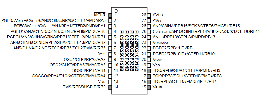
PIC32MX250F128B
SPI
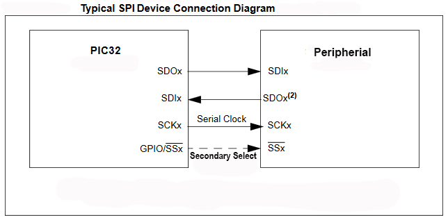
SPI is a very simple, fast, serial control link. There are separate transmit and receive lines, which are full duplex, and a clock line. The PIC32 can transmit 8, 16, or 32-bit buffers at clock speeds up to the peripherial clock rate. The pins used for SDI and SDO can be chosen using the PPS system. See also the Reference Manual Chapter. Typical SPI connections are shown below. Four pins are required: data out, data in, clock, and chip select. There are also specialized modes available: Framed mode will be used for DMA.
During channel setup, you choose
- the SPI frequency prescalar
- clock source -- defaults to PBCLK
(peripheral bus clock)
- configure the data width (8, 16, 32 bits)-- You can change the data width at any time.
- put the PIC in main-mode or secondary-mode
- the clock/data polarity relationship.
Typical control sequence:
- Drop the CS line to start the transaction.
The Secondary Select pin has special function, but you can use any GPIO pin (except in framed mode)
- Load the transmit register. Clock starts automatically and sends the data.
- Wait until SPI done. While waiting you can use the CPU for something else.
At high SPI clock speeds (above a few MHz) it does not make sense to do a context switch or take an interrupt.
- Read the receive register -- every SPI transaction always does a transmit and receive!
- Raise the CS line to end the transaction.
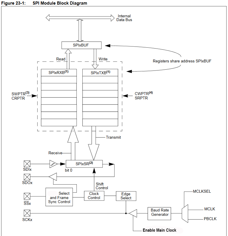
Internally the SPI channel is an independent clocked processor which sends/receives data.
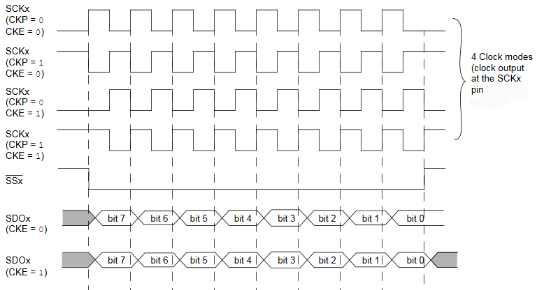
You need to worry about clock polarity and phase. Choosing these is hard because each different manufacturer uses different terminology to explain how their specific chip works. As far as I can tell, Microchip is consistent across their SPI devices. Otherwise I have figure out no better way to figure out polarity and phase than to try all four possibilities and see what works.
Examples
- Framed SPI
An SPI channel can also be run in framed mode. This mode allows the SPI controller to toggle the chip select line, implying that only one peripherial can be attached to that channel, but simplfying program logic. See section 23.3.6 in the reference manual.
Specifically, this feature allows a DMA channel to blast data out to a DAC or other fast device without using an ISR.
The logic might be to set up a DMA channel hardware-triggered by a timer event, with a memory-source (flash or RAM) corresponding to a table of voltages and a memory-destination of the SPI transmit register. The DMA could be operated one-shot for a sound effect, or in auto-repeat mode for a signal generator.
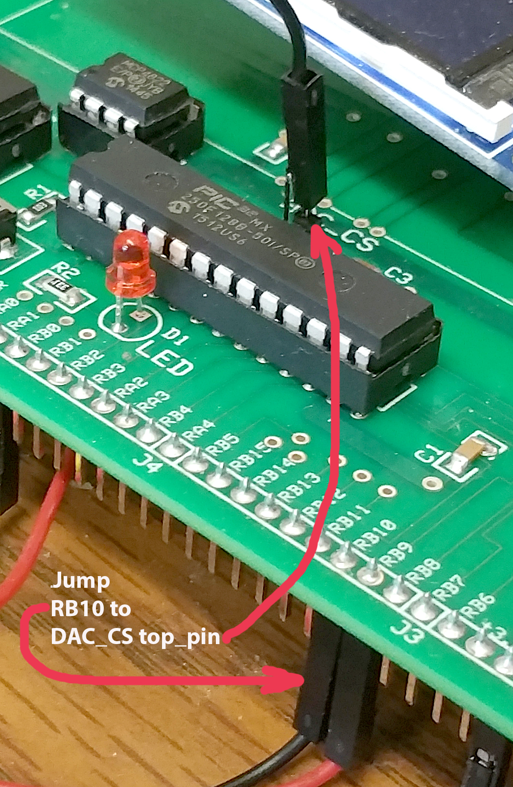
 An example code, running on the big target board uses framed SPI mode, but in an ISR.
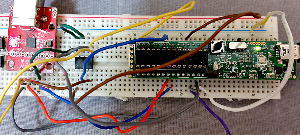
The i/o pin RB10 was jumped to the DAC_CS connector, as shown in the (clickable) image.
The setup code is
SpiChnOpen(SPI_CHANNEL2,
SPI_OPEN_ON | SPI_OPEN_MODE16 | SPI_OPEN_MSTEN | SPI_OPEN_CKE_REV | SPICON_FRMEN | SPICON_FRMPOL, 2);
PPSOutput(2, RPB5, SDO2);
PPSOutput(4, RPB10, SS2);
With the PPS-selected RPB10 used as the hardware secondary-select line, SS2.
(ZIP of project)
-
SPI RAM and DAC
Streaming data from the serial RAM (below) to the MCP4822 DAC is a way to show how to share a SPI channel between two peripherials.
The combined code uses a UART interface to interactively read/write RAM or transfer a RAM data value to the DAC. Only a single byte is transfered, so the DAC value is scaled to 12 bits. The only change to the SPI channel is to have two secondary-select lines, one for the RAM and one for the DAC.
Remember to ground LDAC if you do not need Vouta and Voutb to be synched. (This code shows how to set up the DAC by itself on an SPI channel.)
DAC connections are:
- Serial RAM control
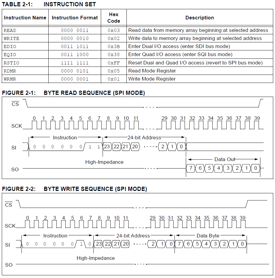
Microchip makes a very nice 1 Mbit serial RAM, organized as 128K of 8-bit words (23LC1024). Access
is controlled by writing a read/write conmmand ORed with a 24 bit address to form 32-bit SPI data. The read/write command occupies the top 8-bits of the 32-bit word. Once an command/address is sent, sequential bytes can read/written using 8-bit transfers. At 20 MHz SPI bit rate, writing the control word (including mode-setting overhead) takes 2.2 microseconds. Each sequential byte read/write takes 0.75 microseconds. The demo code is arranged as a command line interface for testing the RAM connections and read/write logic. As usual, the program requires the protothreads environment. There are functions for read/write a single byte or an array. The RAM defaults to sequential write mode at power-up. This feature is used to write multiple bytes.
RAM Connections are:
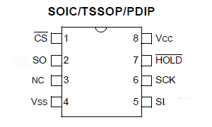
23LC1024 SCK pin 6 to PIC32 pin 26 (SCK2)

    23LC1024 SI pin 5 to PIC32  pin 14 using PPSOutput(2, RPB5, SDO2);

    23LC1024 SO pin 2 to PIC32  pin 9 using PPSInput(3, SDI2, RPA2);

    23LC1024 CS pin 1 to PIC32  pin 4  (port B0)

    23LC1024
HOLD pin 7 must be connected to Vcc (see data sheet)
23LC1024 pin 3 is no connect
(simplified from data sheet -- ignores multiSPI connection)
A bit of timing information from the data sheet.
- NTSC video synthesis and output using SPI
--NTSC video is an old standard, but is still used in North America
for closed circuit TV. It is fairly simple to generate a black/white NTSC signal. Also, the frame buffer for a 1-bit, 256x200 pixel image is only 1600 words (6400 bytes) of RAM.
Chapter 13 of Programming 32-bit Microcontrollers in C: Exploring the PIC32 by Lucio Di Jasio was very useful. I used Di Jasio's method of generating sync pulses using one output-compare unit. Video is sent to the SPI controller using DMA bursts from memory (also similar to Di Jasio), but DMA timing-start control was implemented using another output-compare unit rather than chaining two DMA channels. This allowed easy control of video content timing.
Timer2 is ticking away with an match time equal to one video line time. Ouput-compare 2 is slaved to timer2 to generate a series of pulses at the line-rate. The duration of the OC2 pulses (for vertical sync) is controlled by the Timer2 match ISR in which a simple state machine is running, but the pulse durations are not dependent on ISR execution time. Output-compare 3 is also slaved to timer2 and set up to generate an interrupt at a time appropriate for the end of the NTSC back porch,
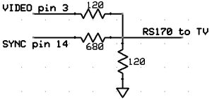
at which time the DMA burst to the SPI port starts. I got best video stability when the core is running at 60 MHz and the peripheral bus running at 30 MHz. The first example is just a bounding ball with some text. The example requires that the ascii character header file be in the project folder. The DAC which combines the SYNC and video signal and adjusts to levels to standard video is:
--The second example is a particle system explosion.
Without doing any space optimization 1500 particles (along with screen buffer) use up memory. All the positions can be updated in every frame. Giving each particle a high initial velocity, and high drag makes a nice cloud.
-- The third example is a particle system fountain, which is a slight modification of the explosion. I optimized the point-draw and one ISR for more efficient execution. Frame update now takes 7.2 mSec. Video.
The overhead for NTSC TV signal generation is about 5 microSec per 63.5 microSec line, or about 8%. You should use this optimized version for an intensive animation.
A small variation makes the particle system fire to the side. Video.
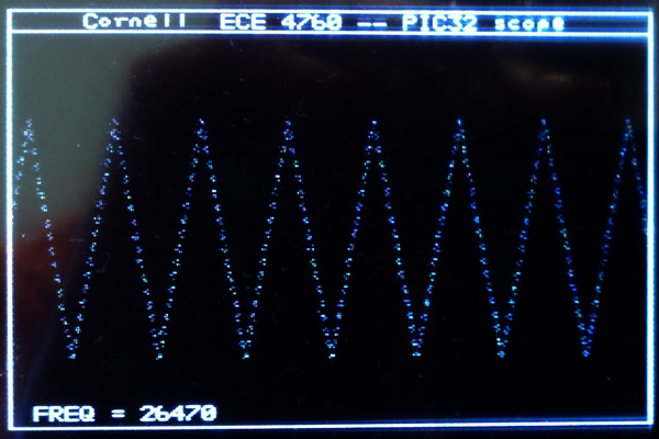
--The fourth example turns on the ADC to make an oscilloscope. The ADC is set up to trigger from the timer3 compare match signal, but without turning on an ISR. A DMA channel transfer is then triggered by the ADC done signal to dump the ADC results to memory at up to 900 Ksamples/sec. This ADC hardware process runs at the same time as the video update hardware process, so video is not disturbed.
CPU load is small so there is time to draw the ADC waveform to the screen. It would be straightforward to add a button state machine for scope control and a FFT. The following image is captured from the NTSC screen and shows the scope running at 900 Ksamples/sec and displaying a frequency estimate. Video is running at 500 Ksamples/sec ADC rate.
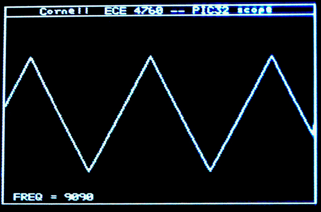
-- The fifth example is a vector variation of the scope. Drawing all the vectors slows the redraw down so that the scope is updated 30 times/sec.
Video is running at 900 Ksamples/sec. Still image below.
- SPI control of a AD7303 DAC
-- It is useful to get a serial channel running for fairly high speed peripherials.
The first device I tried is an Analog Devices AD7303. It is a two channel, 8-bit DAC with buffered voltage output. The channels may be updated simultaneously or separately. Each channel write requires a two-byte transfer to the DAC. The first is a control byte, and the second is the channel data byte. The control byte specifies which channel will be updated as well as the update mode. Each two-byte transfer must be signaled by dropping the voltage on a SYNC pin before the beginning of the transfer, then raising it at the end. Like most microcontrollers the PIC32 SPI interface is simple enough to handle that direct register manipulation is probably the easiest, although the higher level SpiChnOpen function also worked well. The SPI standard supports four clock phases. The microconctoller main-controller has to match the requirements of the secondary peripheral. This is often the most annoying part of getting SPI running. Careful analysis of the slave datasheet is required. The AD7303 requires the main to generate a clock frequency less than 30 MHz, and expects the data to be stable on the the positive clock edge. The required configuration is
SpiChnOpen(spiChn, SPI_OPEN_ON | SPI_OPEN_MODE16 | SPI_OPEN_MSTEN | SPI_OPEN_CKE_REV | SPI_OPEN_CKP_HIGH , spiClkDiv);
or equivalently:
SPI1CON = 0x8560 ; // SPI on, 16-bit, master, CKE=1, CKP=1

      //The SPI baudrate BR is given by: BR=Fpb/(2*(SPI1BRG+1))

      SPI1BRG = 0;  // Fperipheralbus/2
The basic SPI transaction is to start a simultaneous send/receive. On the DAC used here, no useful data is received, but you must do the receive operation to reset the SPI1STATbits.SPIRBF flag. For this application the SPI transaction is
mPORTBClearBits(BIT_0); // start transaction

      SPI1BUF = DAC_cntl_1 | DAC_value ; // write to SPI

      while( !SPI1STATbits.SPIRBF); // check for complete transmit

      junk = SPI1BUF ;   // read the received value (not used by DAC in this example)

      mPORTBSetBits(BIT_0); // end transaction
You clear the SYNC bit, write to SPI1BUF to trigger the hardware trnasmit/receive, wait for it to finish, then do the manditory read and set the SYNC bit. Connections between the two devices are shown below, assuming a certain PPS setup as shown in the code.
| AD7303 |
PIC32 |
| SCLK |
SCK1 is pin 25 |
| DIN |
SDO1 is PPS group 2, map to RPA1 (pin 3) |
| ~SYNC |
PortB.0 (pin 4) |
| not used |
SDI1 is PPS group 2, map to RPB8 (pin 17) |
In addition to the SPI protocol, each different device you attach to the SPI bus has a command syntax which is specific to the device. In this case, the first byte transmitted has the following bit definitions, while the second byte represents the voltage output in straight binary, where binary zero outputs zero volts and binary 0xff outputs Vref..
bit 7 notINT/EXT set to notINT = 0. Use internal Vref

      bit 6 = 0 (not used)

      bit 5 LDAC load and update both channels when set

      bit 4 PDB = 0 pwer down channel B

      bit 3 PDA = 0 pwer down channel A

      bit 2 notA/B = 0 chooses A

      bit 1 CR1=0  control bits modify load mode

      bit 0 CR0=1  set to load A from SR
The actual commands I used here:
Command: Load A from shift register: DAC_cntl_1 = 0b00000001 ;
Command : Load B from SR and and update both outputs: DAC_cntl_2 = 0b00100100 ;
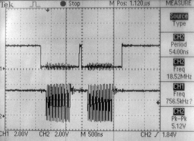
The following image
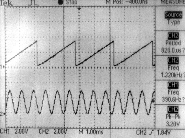
shows the SYNC on the top trace and the SCK1 on the bottom trace. The core frequency and peripheral bus frequency are set 40 mHz. The SCK1 is running at Fpb/2=20 MHz. The total transaction time for the two channels is 2.6 microSec. The second image shows the DAC outputing a DDS sawtooth on one channel and the ADC input on the other at a sampling rate of 100 KHz. Setting the core and peripheral bus to 60 MHz runs the AD7303 at its maximum bus speed and drops the total time to transmit one 16-bit transaction to 850 nS and both channels to 1.75 microSec. The code in the ISR was arranged so that all ISR housekeeping is being done while the SPI hardware does the transmit.
References:
- Beginner's Guide to Programming the PIC32 Paperback by Thomas Kibalo
and more info
- Programming 32-bit Microcontrollers in C: Exploring the PIC32 by Lucio Di Jasio
and more info
- PIC32 Architecture and Programming by Johm Loomis Numb3rs
- Intro to PIC32 architectture
- PIC32 tutorials
- UMass M5 PIC32 tutorials and specifically for the PIC32MX220
- Northwestern University mechatronics design wiki:
- code examples,
- benchmarking,
- Embedded programming on PIC32
- Tahmid's Blog
- chipKit
- Arduino library for PIC32
- Microstick configuration
- project zip
- DSP experiments and more and
- RTOS
- http://www.freertos.org/ and Microchip PIC32 FreeRTOS Reference Designs and MPLABX and ECE443 ref
- TNKernel
- ERIKA Enterprise
- Q-Kernel
- Protothreads by Adam Dunkels
- Protothreads -- similar to Dunkels, but different implementation only for GCC
- MIPS32 docs
- Architecture
- instruction set
- privliged resources
- Microchip Docs
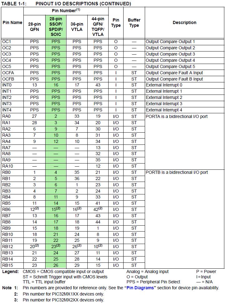
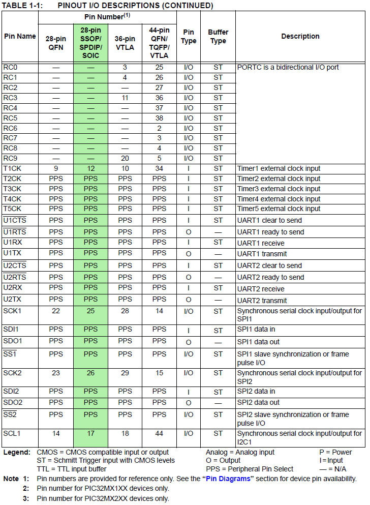
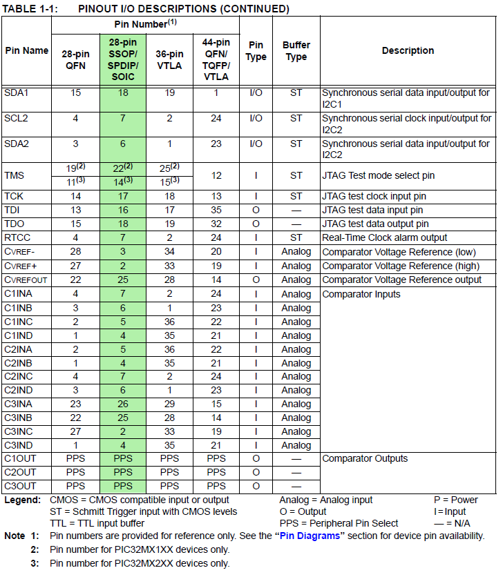
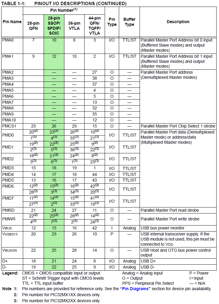
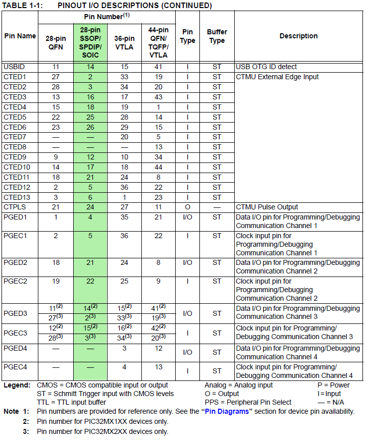
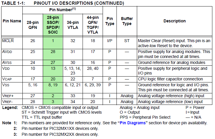
- PIC32MX250F128B PDIP pinout by pin
- PIC32MX250F128B ::: Signal Names=>Pins ::: 1, 2, 3, 4, 5, 6, 7 PDIP highlighted in green (for PPS see next tables)
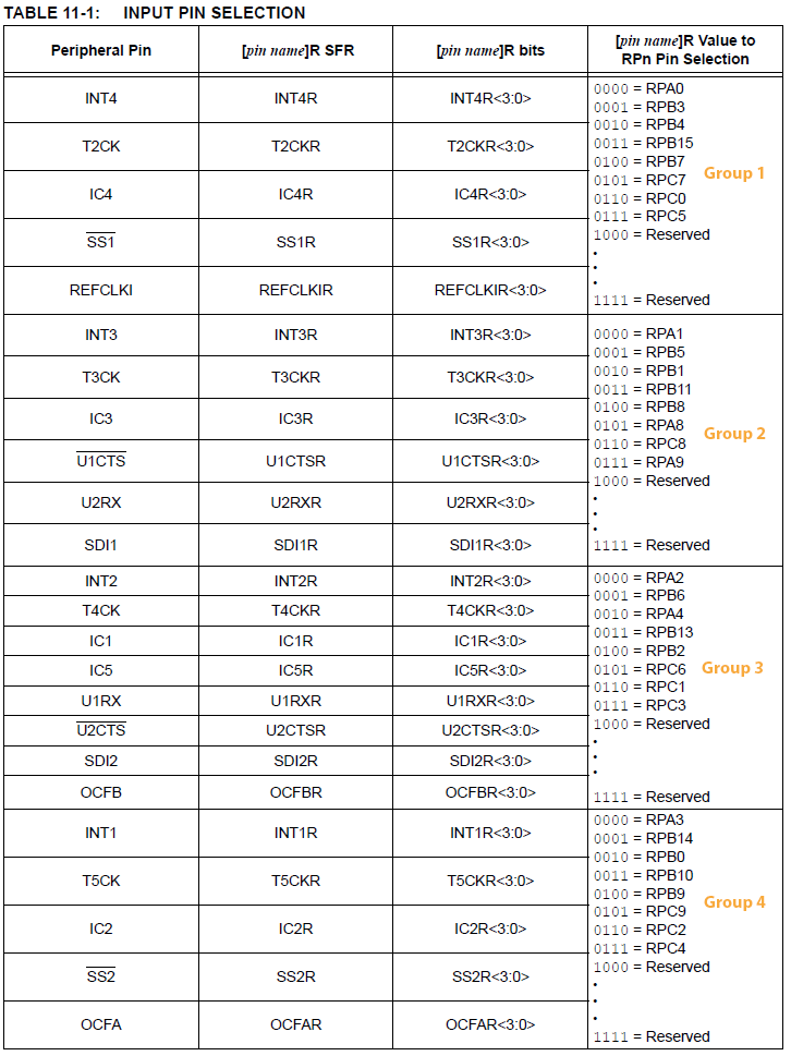
- PIC32MX250F128B Peripheral Pin Select (PPS) input table
example: UART receive pin ::: specify PPS group, signal, logical pin name
PPSInput(2, U2RX, RPB11); //Assign U2RX to pin RPB11 -- Physical pin 22 on 28 PDIP
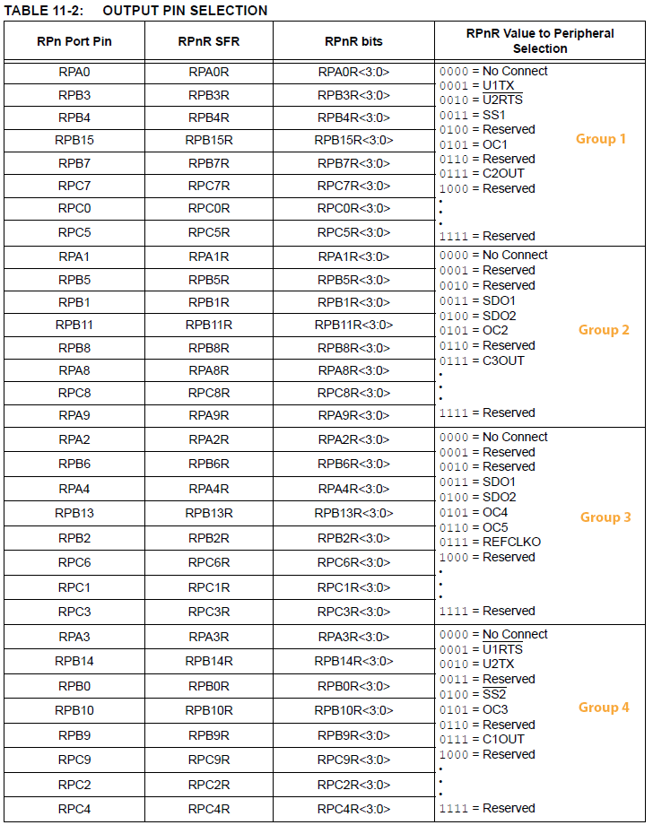
- PIC32MX250F128B Peripheral Pin Select (PPS) output table
example: UART transmit pin ::: specify PPS group, logical pin name, signal
PPSOutput(4, RPB10, U2TX); //Assign U2TX to pin RPB10 -- Physical pin 21 on 28 PDIP
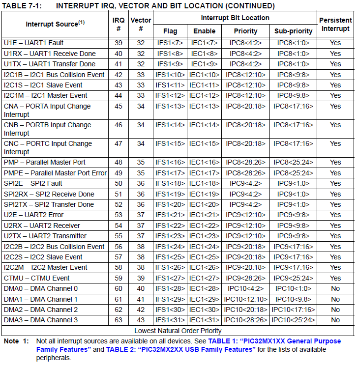
- PIC32MX1XX/2XX Interrupt Table 1, 2 and int_1xx_2xx.h -- interrupt IRQ names and vector names
- plib.h names of peripherial header files
-----------------------------------------------------------------
- Getting started with PIC32
- MPLABX IDE users guide
- PICkit3 Users Guide and poster
- 32_bit peripherials library
- 32 bit language tools and libraries including C libraries, DSP, and debugging tools
- XC32 Compiler Users Guide
- microstickII pinout
- PIC32 reference manual
and more from Northwestern University mechatronics design wiki, PIC32 page
- MIPS-M4K Core
- 2xx_datasheet
- Microchip doc site on this page choose
Documentation from the left column.
The Reference Manual is particuarly useful
- USB Embedded Host Stack
- chipKIT (PIC32 arduino library)
- code examples (choose PIC32 in product family dropdown)
- code libraries (choose PIC32 in product family dropdown)
- application notes (choose PIC32 in panel)
- Harmony for PIC32 -- docs --
- Microchip TCP/IP Stack Application Note
- External Refs back to this work
- http://dangerousprototypes.com/2014/07/15/pic32-oscilloscope/
- http://hackedgadgets.com/2014/07/14/pic32-oscilloscope/
Copyright Cornell University
July 16, 2020
 An example code, running on the big target board uses framed SPI mode, but in an ISR.