Cornell University ECE4760
Analog/Digital Converter
PIC32MX250F128B
ADC
There are a huge number of options for the ADC. Some options are outlined below.
See also Reference manual, chapter 17.
ADC hardware:
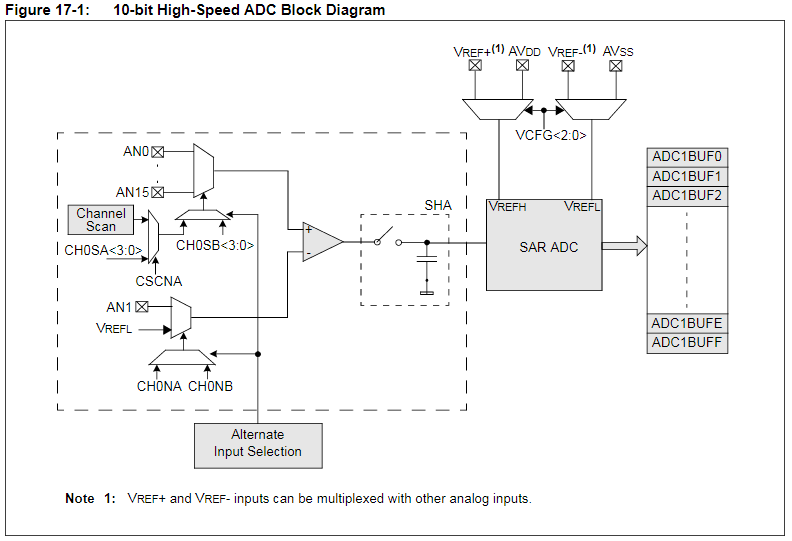
The PIC32 10-bit Analog-to-Digital Converter (ADC) includes the following features:
• Successive Approximation Register (SAR) conversion
Up to about 1 MHz, with 10-bit resolution
To get to 1 MHz you cannot sample in an ISR, but must use DMA
• Up to 16 analog input pins -- But 9 inputs on our package.
AN0-5 and
AN9-11
The analog inputs are connected through two multiplexers to one SHA.
The analog input multiplexers can be switched between two sets of analog inputs between conversions.
As seen above, measurements are single-ended,
except for option ofl using AN1 for negative differential input.
• Internal voltage references with the option of external voltage reference input pins
• One unipolar differential Sample-and-Hold Amplifier (SHA)
• Automatic Channel Scan mode
The Analog Input Scan mode sequentially converts user-specified channels.
A control register specifies which analog input channels will be included in the scanning sequence
• Selectable conversion trigger source
Auto conversion, software trigger, timer3 period match trigger,
int0 trigger
• 16-word conversion result buffer with selectable Buffer Fill modes
• Eight conversion result format options
16 bit, 32 bit, signed/unsigned, fractional
(signed useful for differential input)
• Generate interrupt or trigger DMA cell transfer on ADC complete event.
The ADC can be set up to capture several channels before an
ADC complete event is generated.
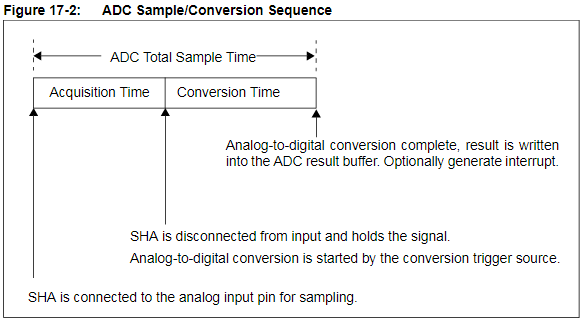
Terminology for ADC timing:
Examples
- Converting a analog input in a thread.
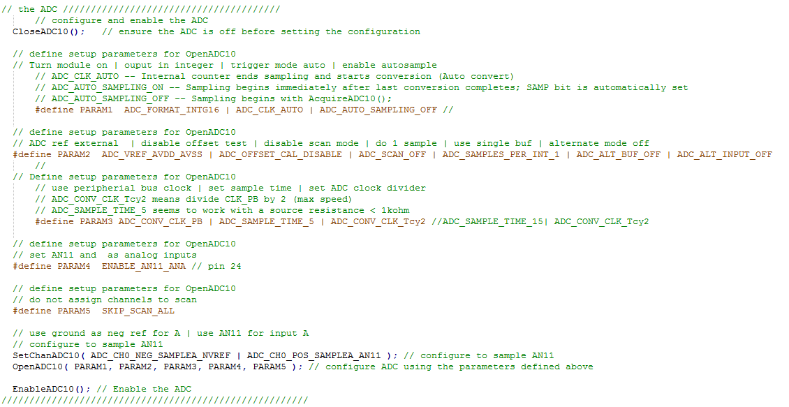
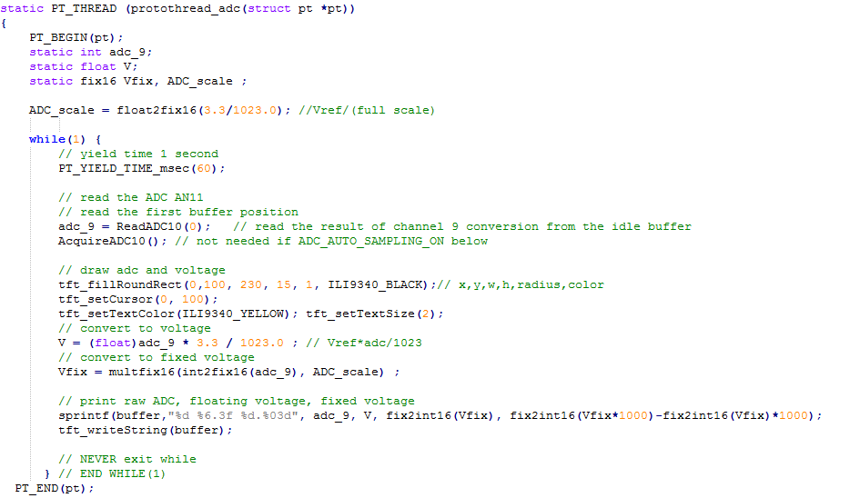
This example code sets up an ADC read on one pin, scales the value to a voltage, and prints it on the TFT display.
The analog input converted is AN11 on i/o pin RB13.
The setup code for the ADC, and the thread that reads it.
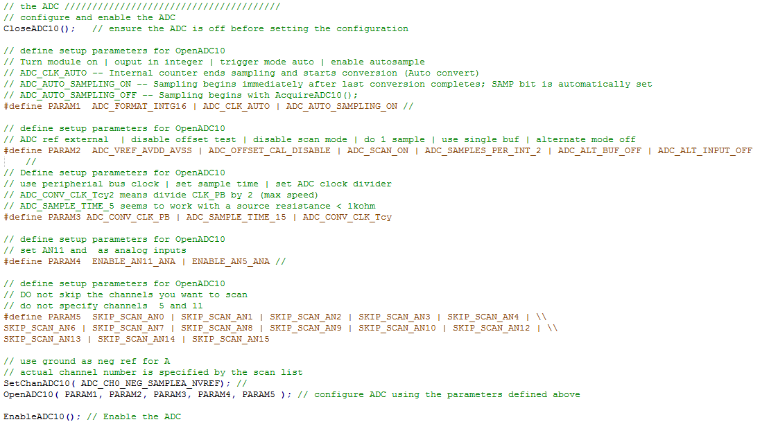
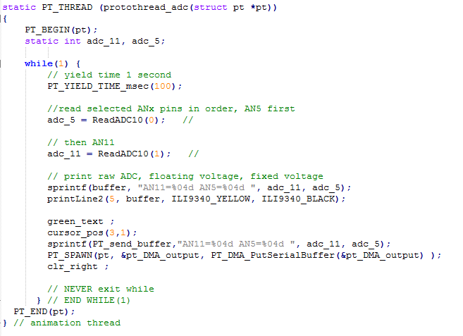
- Converting multiple channels in a thread.
The ADC hardware has the ability to scan multiple analog inputs and store all of the scanned digital values into a hardware-defined array (see first figure).
To do this you must set ADC_AUTO_SAMPLING_ON. A thread can then read all the stored values. (Code)
The following older examples use a simple setup with no threader.
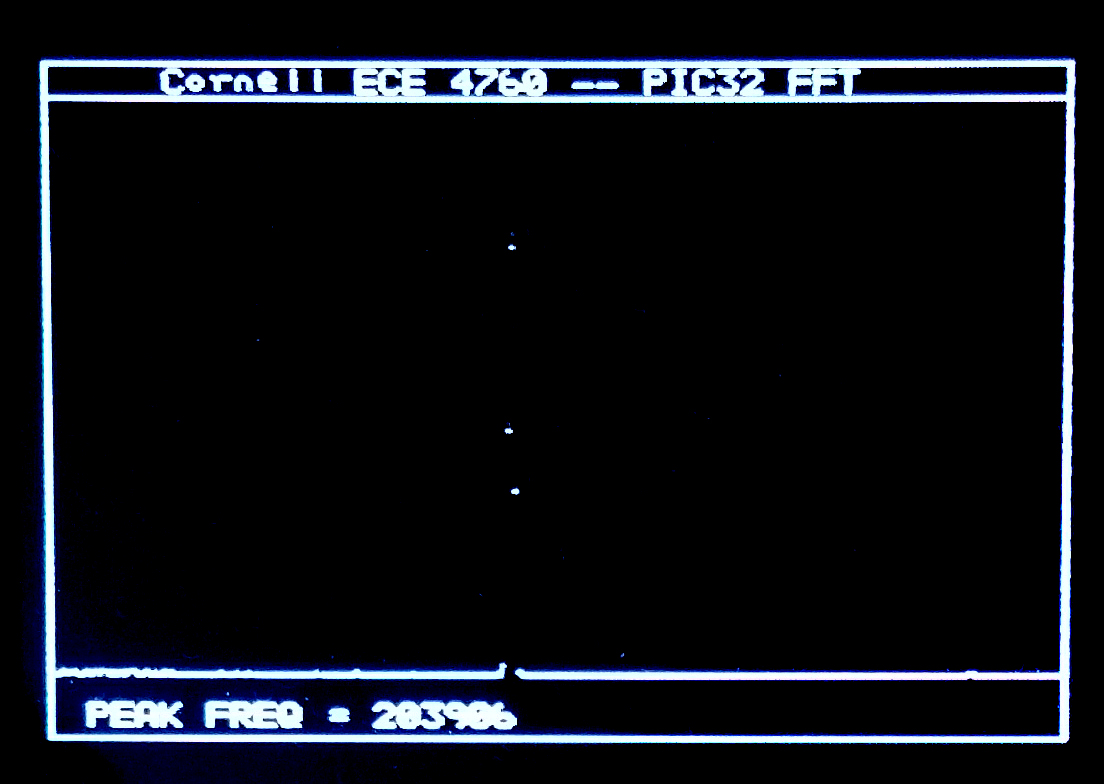
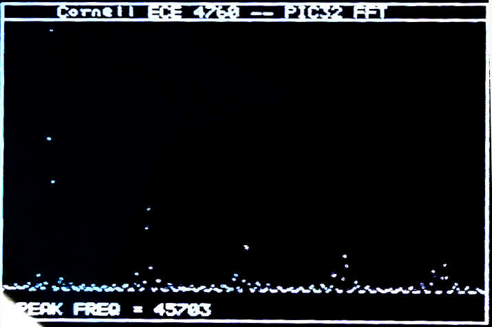
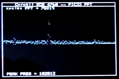
- ADC input using DMA at 900 KHz: Spectrum analyser with video output
The TV framework described below was used as a spectrum analyser by adding a fixed point FFT routine. The routine works in 16:16 fixed format. A 512 point complex FFT takes 410,000 cpu cycles (with no optimization) or about 6.8 milliseconds. If we include the time to Hanning window the signal and compute the magnitude of the complex output, the process takes 454,800 cpu cycles (with no optimization), or about 7.6 milliseconds. Running the compiler at optimization level 1 (highest free compiler level) reduces the number of cpu cycles to 146,000, or about 2.4 milliseconds for Hanning-FFT-magnutude calculation. The two images show a sine signal and a square wave captured at 900,000 samples/sec. There is some aliasing of the square wave so the peaks are not clean, but you can see the 1/f spectrum. The magnitude of the FFT is approximated as |amplitude|=max(|Re|,|Im|)+0.4*min(|Re|,|Im|). This approximation is accurate within about 4%.
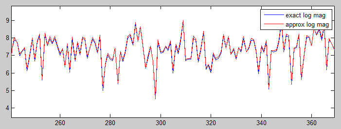
Taking the log of the magnitude using a fast approximation
(Generation of Products and Quotients Using Approximate Binary Logarithms for Digital Filtering Applications, IEEE Transactions on Computers 1970 vol.19 Issue No.02) gives more resolution at lower amplitudes( code). Evaluation of the algorithm as a matlab program is here. The following images give the matlab comparison of exact and approximate log for noise, and a sinewave FFT on the PIC32.
- ADC performance using ISR at 500 KHz
-- The
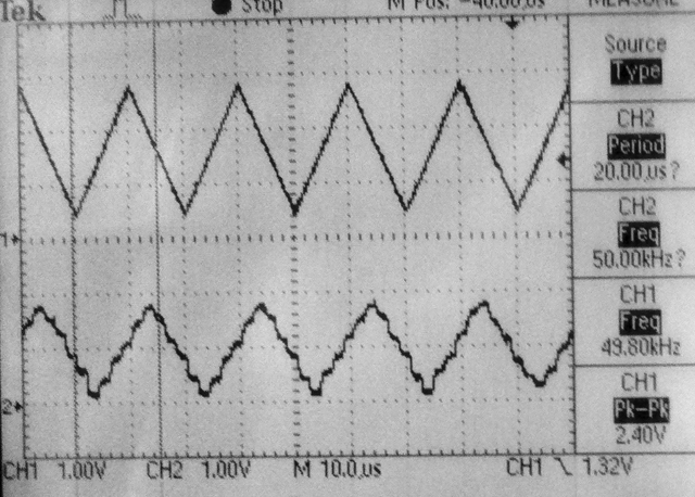
PIC32 has a 10-bit ADC which runs up to 1 MHz sample rate, although the first example is limited to a little more than 500kHz because sampling is controlled by an ISR (see below for interrupt perfomance). The first example samples one channel, with most ADC features disabled. The ADC_CLK_AUTO is turned on so that conversion immediately follows sample-aqusition, but aquisition is started manually in the ISR and goes into one slot of the buffer array where it is immediately copied into the Vref DAC for output to the scope. The first image shows the signal generator input to AN4 on channel one and the limited resolution Vref DAC on channel two. The triangle wave is set to 50 kHz. Since the sampling rate is 500 kHz there are 10 samples on each cycle, probably about the limit for sampling. There appears to be about 1.5 samples of phase delay at the positive peak, but less at the negative peak because of nonlinear loading effects noted in the Vref DAC section.
--
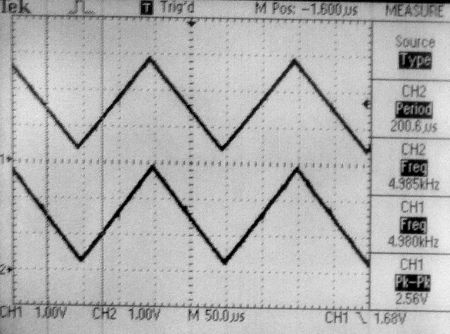
The ADC specification (search on TAD in the datasheet) says that for a low Z source (<500 ohms) the ADC bit-clock period must be >65 nSec and the ADC sample period must be >132 nSec. At peripheral bus clock of 40 MHz (period 25 nSec), ADC_SAMPLE_TIME_6 should work for the sample period (150 nSec) and ADC_CONV_CLK_Tcy2, while a little fast (50 nSec), seems to work for the ADC clock.A safer code turns ADC_AUTO_SAMPLING_ON so that the ADC runs as fast as possible makes it possible to sample at 500 KHz using ADC_CONV_CLK_Tcy, which exceeds the minimum bit-clock period time by setting the bit sample time to 100 nSec. Hooking up a higher quality DAC
( 4116R-R2R-253LF resistor array) gives 8-bit resolution and allows accuracy testing of the ADC. The DAC resistor array is mapped to port B bits (lsb) 0-5 and bits 14 and 15 (msb). These port signals are pins (from lsb to msb) 4,5,6,7,11,14,25,26. The mapping does not use port B, bit-6 because the 28 pin PDIP package does not support it (see datasheet Table 1.1). Some care is needed to prevent the digital signals from coupling to the analog output. The second image shows the output from the 8-bit DAC on the bottom trace with small coupling artifacts near the 50% point.
-- Changing the core clock to 60 MHz and the peripheral bus clock to 30 MHz allows a ADC bit-clock period of 66 nSec, exactly the minimum for the bit-clock. With ADC_AUTO_SAMPLING_ON and with ADC_SAMPLE_TIME_5 and ADC_CONV_CLK_Tcy2 the system can sample at 750 KHz with a few cycles left over for main.
Oscillator configuration:
#pragma config FNOSC = FRCPLL, POSCMOD = HS, FPLLIDIV = DIV_2, FPLLMUL = MUL_15, FPBDIV = DIV_2, FPLLODIV = DIV_1
#pragma config FWDTEN = OFF
#pragma config FSOSCEN = OFF, JTAGEN = OFF
// core frequency we're running at // peripherals at 30 MHz
#define	SYS_FREQ 60000000
References:
- Beginner's Guide to Programming the PIC32 Paperback by Thomas Kibalo
and more info
- Programming 32-bit Microcontrollers in C: Exploring the PIC32 by Lucio Di Jasio
and more info
- PIC32 Architecture and Programming by Johm Loomis Numb3rs
- Intro to PIC32 architectture
- PIC32 tutorials
- UMass M5 PIC32 tutorials and specifically for the PIC32MX220
- Northwestern University mechatronics design wiki:
- code examples,
- benchmarking,
- Embedded programming on PIC32
- Tahmid's Blog
- chipKit
- Arduino library for PIC32
- Microstick configuration
- project zip
- DSP experiments and more and
- RTOS
- http://www.freertos.org/ and Microchip PIC32 FreeRTOS Reference Designs and MPLABX and ECE443 ref
- TNKernel
- ERIKA Enterprise
- Q-Kernel
- Protothreads by Adam Dunkels
- Protothreads -- similar to Dunkels, but different implementation only for GCC
- MIPS32 docs
- Architecture
- instruction set
- privliged resources
- Microchip Docs
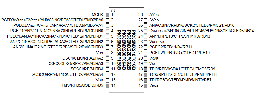
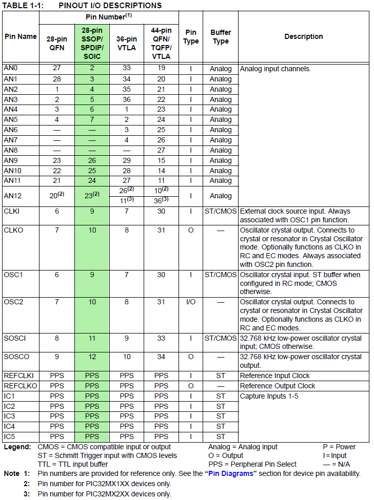
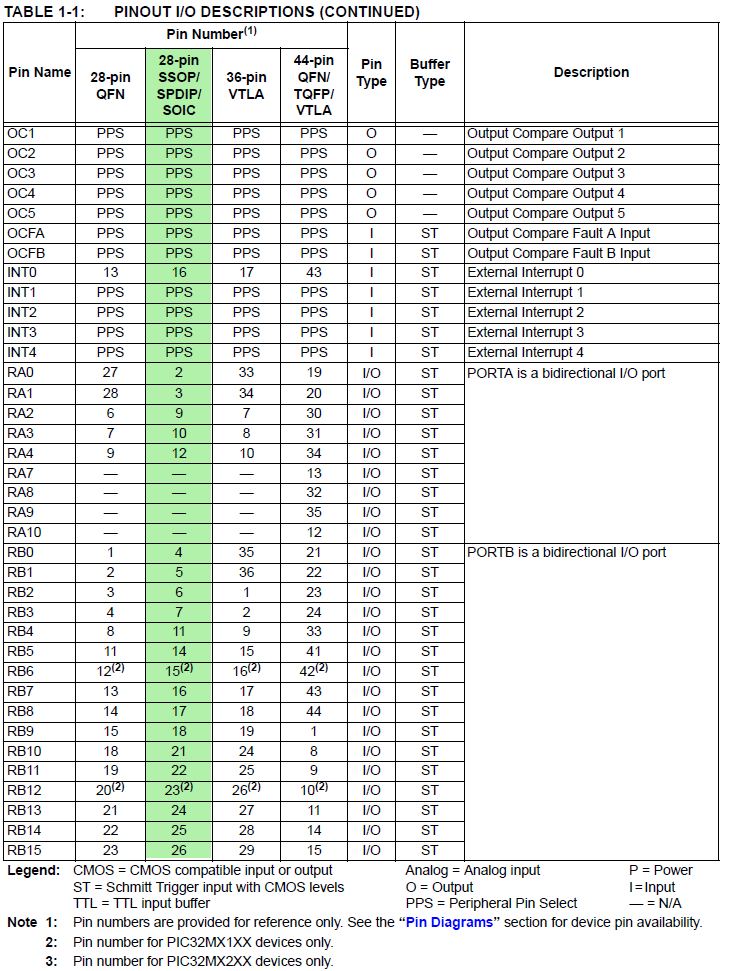
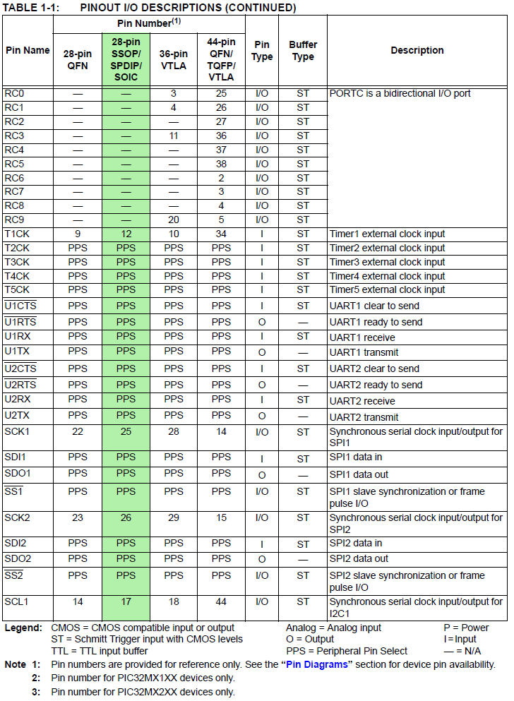
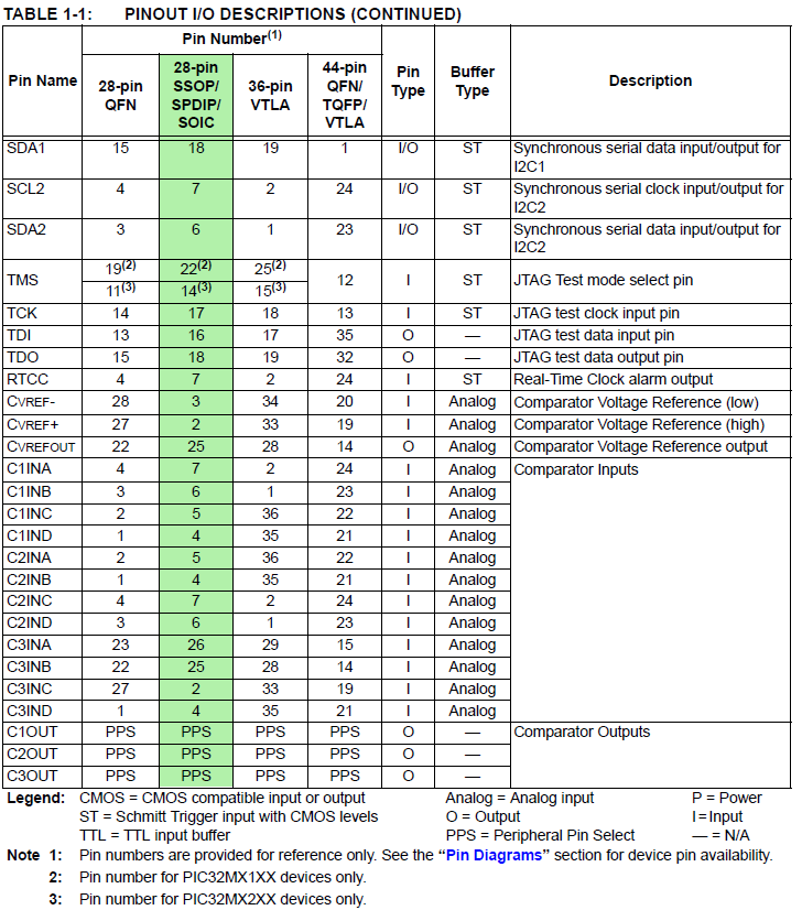
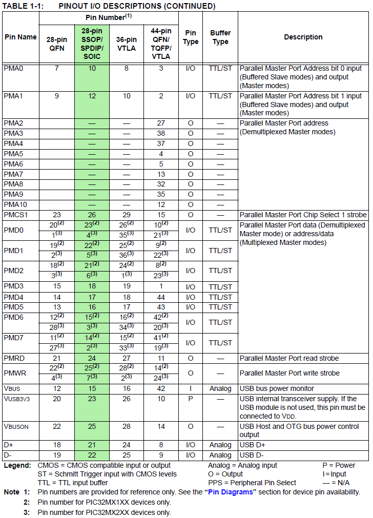
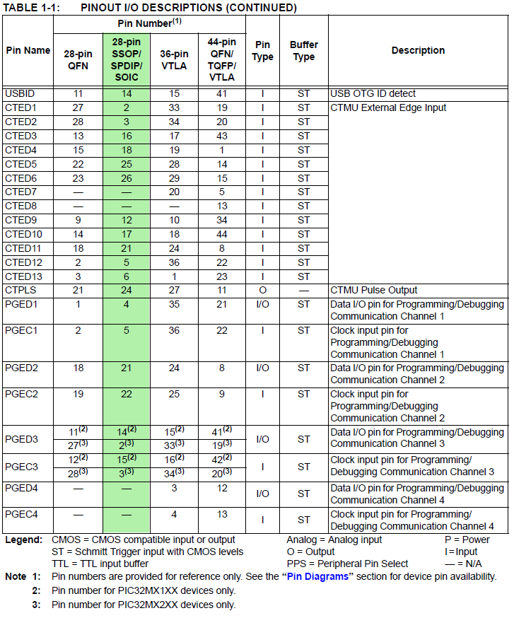
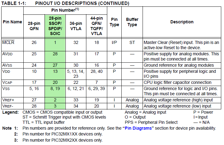
- PIC32MX250F128B PDIP pinout by pin
- PIC32MX250F128B ::: Signal Names=>Pins ::: 1, 2, 3, 4, 5, 6, 7 PDIP highlighted in green (for PPS see next tables)
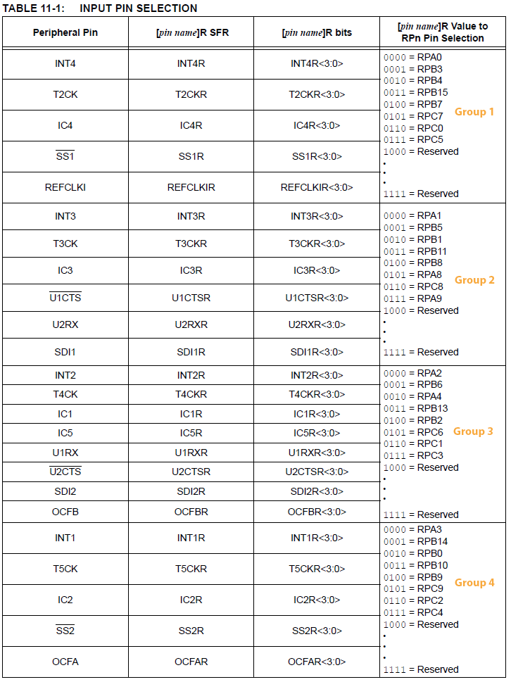
- PIC32MX250F128B Peripheral Pin Select (PPS) input table
example: UART receive pin ::: specify PPS group, signal, logical pin name
PPSInput(2, U2RX, RPB11); //Assign U2RX to pin RPB11 -- Physical pin 22 on 28 PDIP
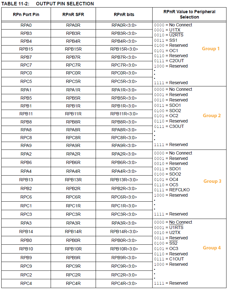
- PIC32MX250F128B Peripheral Pin Select (PPS) output table
example: UART transmit pin ::: specify PPS group, logical pin name, signal
PPSOutput(4, RPB10, U2TX); //Assign U2TX to pin RPB10 -- Physical pin 21 on 28 PDIP
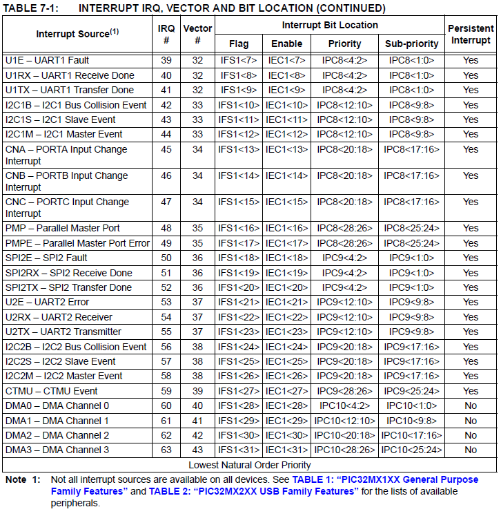
- PIC32MX1XX/2XX Interrupt Table 1, 2 and int_1xx_2xx.h -- interrupt IRQ names and vector names
- plib.h names of peripherial header files
-----------------------------------------------------------------
- Getting started with PIC32
- MPLABX IDE users guide
- PICkit3 Users Guide and poster
- 32_bit peripherials library
- 32 bit language tools and libraries including C libraries, DSP, and debugging tools
- XC32 Compiler Users Guide
- microstickII pinout
- PIC32 reference manual
and more from Northwestern University mechatronics design wiki, PIC32 page
- MIPS-M4K Core
- 2xx_datasheet
- Microchip doc site on this page choose
Documentation from the left column.
The Reference Manual is particuarly useful
- USB Embedded Host Stack
- chipKIT (PIC32 arduino library)
- code examples (choose PIC32 in product family dropdown)
- code libraries (choose PIC32 in product family dropdown)
- application notes (choose PIC32 in panel)
- Harmony for PIC32 -- docs --
- Microchip TCP/IP Stack Application Note
- External Refs back to this work
- http://dangerousprototypes.com/2014/07/15/pic32-oscilloscope/
- http://hackedgadgets.com/2014/07/14/pic32-oscilloscope/
Copyright Cornell University
September 30, 2019