Here we will take a deep dive into our hardware and software design of the system. We will discuss our design considerations and then go through the modules used in RTL. Our software is fairly simple, so the emphasis of this section will be RTL. Our source code will be made available under MIT license.
The goal of this section is to provide enough detail such that an experienced RTL designer could replicate our design by reading this section. One would also need to understand how the HPP model works. It is impossible to put everything in our code into words. After all, if the source code is available, most engineers would prefer reading code instead of paragraphs. We will do our best here.
HW Details
Design Requirements
Here are some design specifications we came up with before start coding:
- Each pixel on the 640 × 480 VGA display should represent a grid cell, containing up to 4 particles or being an obstacle.
- Particle movements should be smooth and synchronized. RTL has to finish calculations for all the grids in one frame.
- We are aiming for 60 frames per second.
Design Considerations
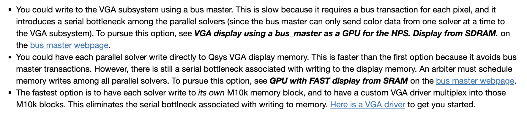
VGA Bandwidth
Hunter (the course instructor) mentioned here that there are three ways to send data into the VGA buffer for display (see picture below). In order to achieve 60 frames per second on a 640 × 480 VGA display, the third one (custom VGA driver) is the only option. We used Hunter's code with some modifications.
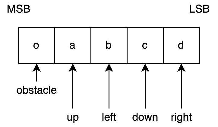
Grid Representation
Each grid could contain up to 4 particles. Particles in each of the four directions could be either present or not (1-bit information). In addition, we need 1 more bit to represent whether or not a grid is an obstacle. Therefore, we need 5 bits in total. Here is a picture showing what each bit represents.
Parallel Computation
Cellular automaton is embarrassingly parallel. Our parallelization scheme is to calculate the next state of one column of pixels (or grids) on the VGA screen in parallel. This way, we will achieve 480X speed up compared to calculating the grids one by one.
We did not choose to do parallelization in the horizontal direction (compute a row of grids in parallel) because we want to be conservative at first to potentially make synthesis easier on the FPGA. We also believe that this design is sufficient to meet our design requirement with some back-of-envelope calculations. Iterating over the whole screen should take ~640 cycles. Doubling this number to account for both collision and propagation would mean ~1300 cycles. This is a very short time when the design is running at 50 MHz.
There are other cellular automaton schemes that has a grid-like design, and can achieve higher speedup. But we do want to keep the design simple to make sure we meet the project timeline.
Memory Limitation
Performing computation of the whole column together implies 480 parallel reads/writes. This is not feasible because there are only 390 M10K blocks, each having 1R1W dual port. Further investigation shows that these M10K blocks also has 10-bit × 1K configuration. Because computation of a column of grid is synchronized, this means we can store the states of two grids together in one M10K address. Each M10K block will store the state of two rows on the VGA screen, and each will store 640 unit of "two grids' state." Perfect.
M10K Read Share & Timing Requirements
But here is another issue. When the model is performing computation, it will be reading and writing to the M10K blocks. However, the VGA driver will also be sending requests into the M10K blocks for the grid information in position (x,y). There may be a smart way to arbitrate between VGA driver requests and model evolution, but we found a more straight-forward solution.
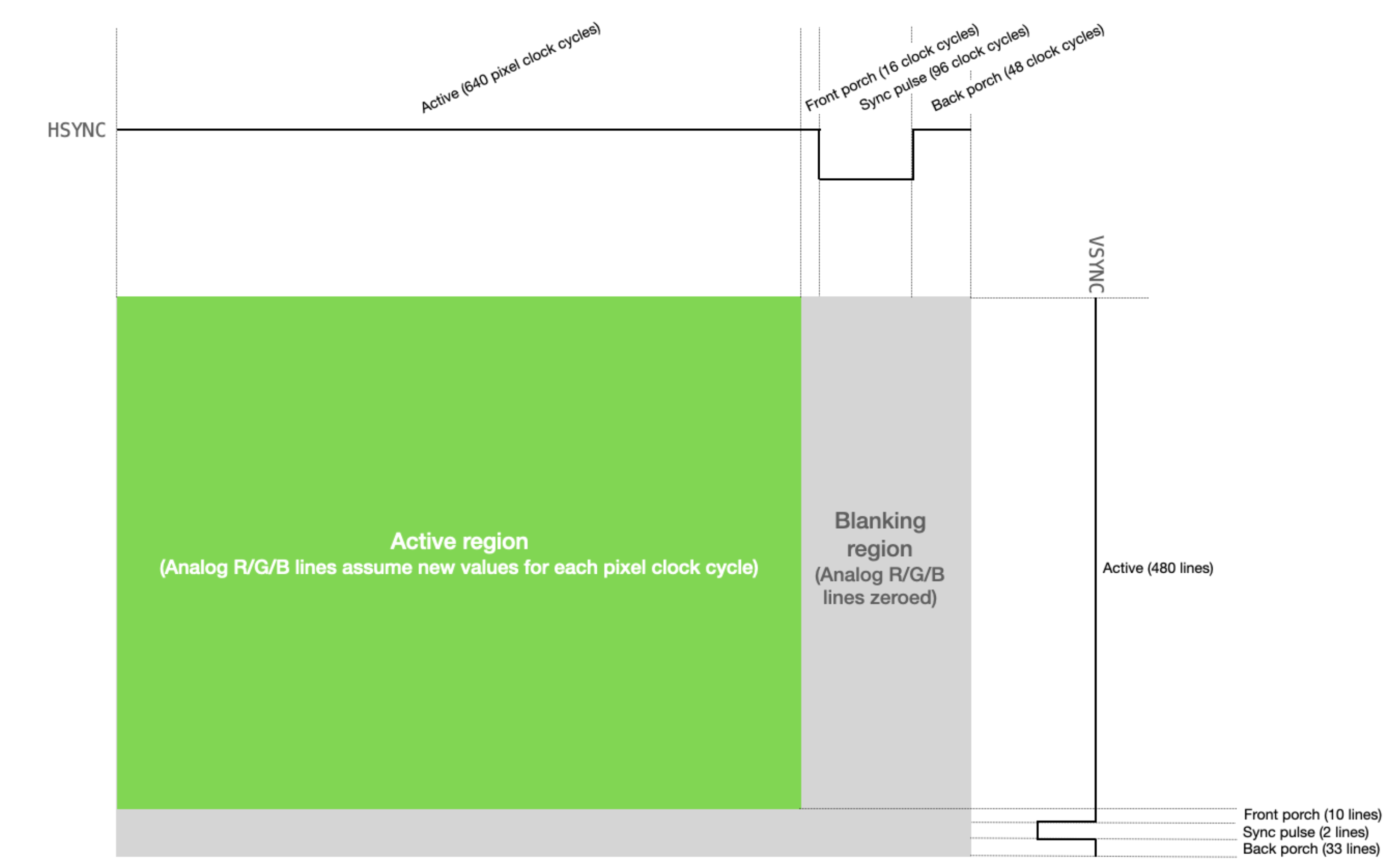
A diagram of the VGA standard is shown below. The VGA driver scans by row. It iterates over one row, and moves to another. Within the active region, the VGA driver sends out next_x and next_y signals trying to get the color for that pixel. However, we can see that the VGA driver is inactive in the bottom 45 lines. If we multiply that number by 800 clock cycles for a row, then there is 36000 cycles at 25 MHz (VGA driver clk freq), which is 72000 cycles at 50 MHz. If our RTL can finish rendering a frame within 72000 cycles, then we can avoid data racing and achieve frame synchronization at the same time.
This is what we do, and this is why there is this enter_v_front signal from the VGA driver to our top level design, which will be asserted for 2 cycles when VSYNC enters front porch.
Remember, with our design, rendering a frame will only take ~1300 cycles, that is 1.8% of 72000 cycles. This still leaves a lot of room for extra states for HPS interactions where overwriting grid information is needed.
System Level
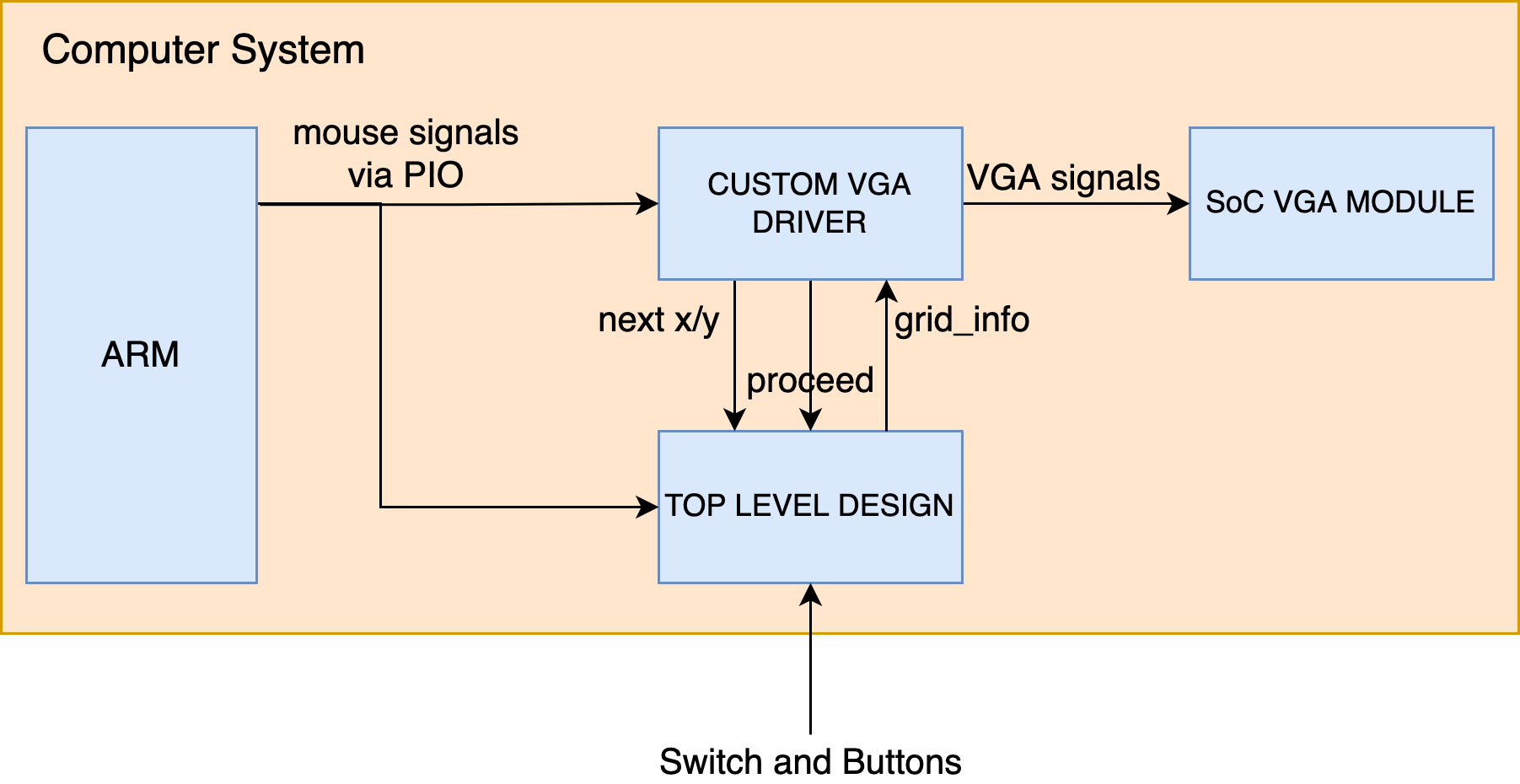
The whole computer system contains both the ARM and our custom RTL design. The ARM (or HPS, whatever you like to call it) uses parallel i/o ports to transmit mouse signals to the RTL design. There is the modified version of Hunter's VGA driver. The VGA driver sends out requests when it is in the active region into the top level design, and the top level design sends back the grid state. The VGA driver module will map the grid's state into 8-bit RGB color. There is this proceed signal (or enter_v_front in the actual code) sent from the VGA driver to the top level design. This signal is assert high when the VGA driver enters the verticle front porch, meaning that the top level design can now use the read ports of the M10K blocks. The top level design is responsible for updating the grids' states. There is also the SoC VGA module, which is controlled by the custom VGA driver.
VGA Driver
As mentioned before, the VGA driver is modified from Hunter's VGA driver. We added the enter_v_front signal, the color mapping for the grids' states, and the square that shows where the mouse pointer is at. The code snippet below should help.
wire [2:0] num_particles;
assign num_particles = grid_info[0] + grid_info[1] + grid_info[2] + grid_info[3];

wire [23:0] color_in;
assign color_in = (((next_x == ptr_x_lo || next_x == ptr_x_hi) && (next_y >= ptr_y_lo && next_y <= ptr_y_hi)) || ((next_y == ptr_y_lo || next_y == ptr_y_hi) && (next_x >= ptr_x_lo && next_x <= ptr_x_hi))) ? {8'd0, 8'd255, 8'd0} // draw mouse boundary
                : (grid_info[4] == 1'b1)  ? {8'd255, 8'd168, 8'd54}
                : (num_particles == 3'd0) ? {8'd2, 8'd30, 8'd30} // no particle/background
                : (num_particles == 3'd1) ? {8'd34, 8'd148, 8'd145} // 1 particle
                : (num_particles == 3'd2) ? {8'd62, 8'd178, 8'd168} // 2 particles
                : (num_particles == 3'd3) ? {8'd116, 8'd230, 8'd217} // 3 particles
                : (num_particles == 3'd4) ? {8'd195, 8'd255, 8'd248}   // 4 particles
                : 24'd0;
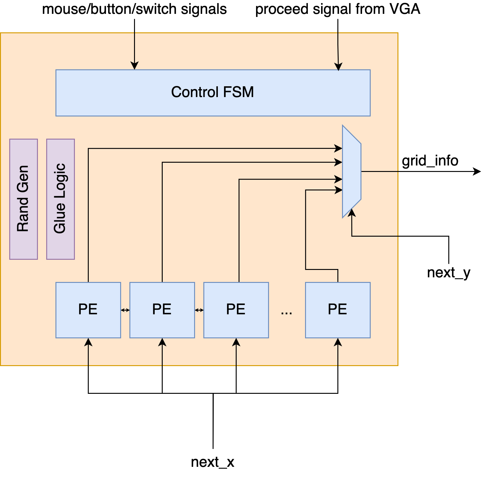
Top Level
The top level design contains everything needed to run the cellular automaton. There is this carefully designed control finite state machine. The state machine orchestrates all the multiplexing of signals, and calculates M10K addresses that are used by the processing elements (PEs). All the external config signals go into the FSM. The enter_v_front/proceed signal also goes into the FSM.
There is a random number generator (a linear feedback shift register we got from Bruce's old code) and some glue logic, but all the heavy-liftings are done by the PEs. Each PE is responsible for calculating two vertical neighboring grids. That is 240 PEs in total. These PE are also connected into a row. The reason is that each grid needs information from its four neighboring grids in the propagation phase.
PE Level
Below is the block diagram of a PE. A PE contains two collision modules. Collision only takes the current state as an input, and it calculates the next state within a cycle. Collision is resolved only by the current state and is not affected by neighbording cells. Each collision module is responsible for the calculation of one grid. The collision module also has an artist mode. What it does is to let obstacles generate new particles. Activation of the artist mode would create unexpected beautiful effects.
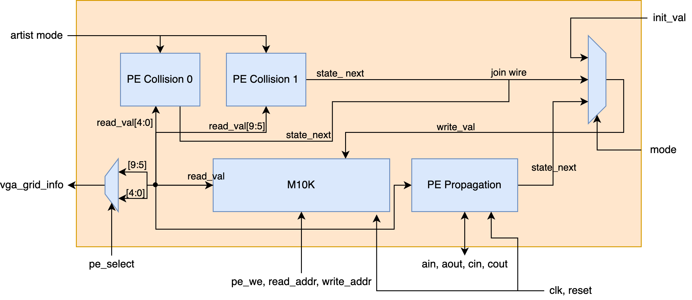
There is one propagation module. The propagation module is responsible for the propagation phase. Each propagation module is responsible for the calculation of two grids. Because the calculation of propagation needs information from neighboring grids, it takes ain, cin from adjacent cells, and generates aout, cout. This is also combinational logic.
There is also the M10K block that is responsible for storing all the states in the two grids that this PE is responsible for. pe_we, read_addr, write_addr are controlled by the FSM. read_val is wired to vga_grid_info (response to VGA requests for grid info), collision modules, and the propagation module. There is a mode input (controlled by FSM) that decides what should be written back to the M10K module.
The PE has four modes:
- Collision mode: outputs from the collision modules are wired to M10K
write_val. - Propagation mode: outputs from the propagation modules are wired to M10K
write_val. - Init/Mouse Overwriting mode: input
init_valfrom the FSM are wired to M10Kwrite_val. This allows the FSM to overwrite information in the M10K. - VGA read mode: In this mode,
pe_weof the M10K block is disabled.read_addris set by the FSM, and the signalpe_selectchooses whether the upper grid or the lower grid is wired out.
PE Collision
We got the very efficient collision algorithm from this website. We modified the algorithm to fit into Verilog (originally in C). The code snippet below should explain everything.
assign change = (a_top & c_bottom & ~(b_left | d_right)) | (b_left & d_right & ~(a_top | c_bottom));

wire K_a, K_b, K_c, K_d; // temp vars
assign K_a = a_top ^ change;
assign K_b = b_left ^ change;
assign K_c = c_bottom ^ change;
assign K_d = d_right ^ change;
Because a grid could be an obstacle, we need the logic to resolve obstacles as well. The code snippet below for the up direction should make sense.
assign a_out = (obstacle && K_c) ? K_c
: (obstacle && K_a && ~artist_mode) ? 1'b0
: K_a;
PE Propagation
The propagation module has nothing fancy. It is simply a matter of careful wiring to meet the rules of the HPP model. However, one thing to note is that our PEs will be sweeping from the left of the screen to the right side of the screen. To generate the state of the current column (suppose column N), the module needs information of the column that is to the right, and the column that is to the left of N, namely N+1 and N-1. This is accomplished by having two states cached inside the propagation module like this.
reg [9:0] prev_state;
reg [9:0] prev_prev_state;

always @(posedge clk) begin
    if (!reset) begin
        prev_state <= 10'd0;
        prev_prev_state <= 10'd0;
    end else begin
        prev_state <= right_state;
        prev_prev_state <= prev_state;
    end
end
The input right_state comes directly from the M10K module. That is the N+1 column. prev_state stores the state of column N, and prev_prev_state stores the state of column N-1. Note that N is the column that the propagation module is working on in this cycle, and the propagation module will generate the updated state of N by the end of this cycle, which will be written into the M10K module.
State Machine
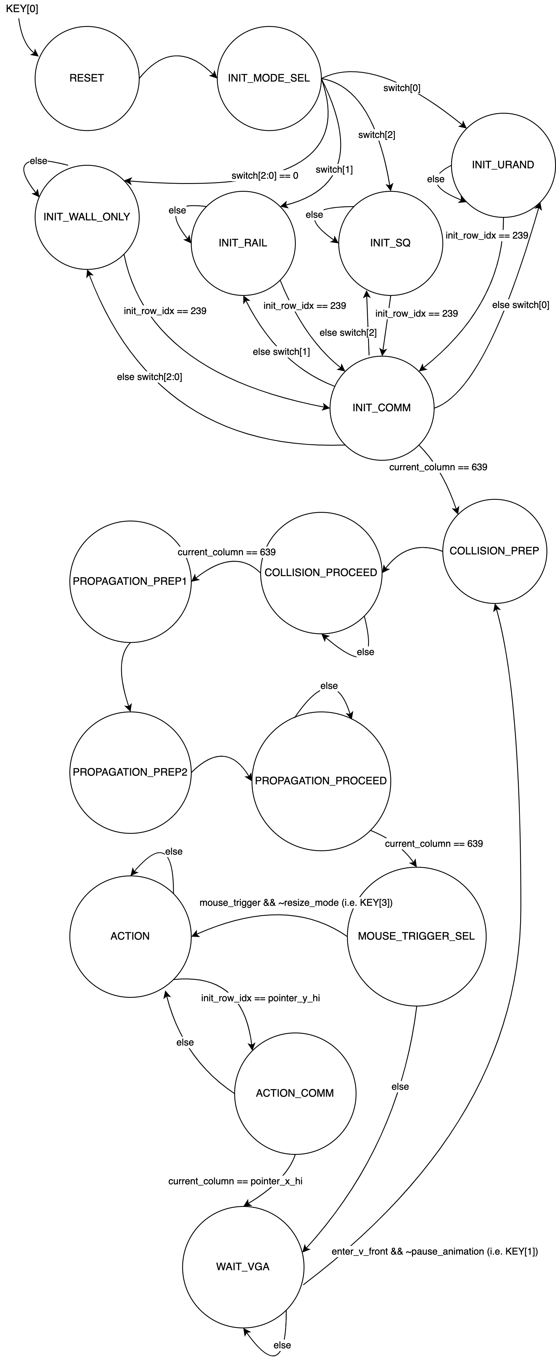
Below is a diagram of the finite state machine transition. Upon KEY[0] is pressed, the FSM goes to the RESET state. It then enters the INIT states. Depending on the configuration of the first 3 switches, it enters different INIT states. init_row_idx and current_column are first set to 0.
Let's call INIT_WALL_ONLY, INIT_RAIL, INIT_SQ, and INIT_URAND as init pattern states. These init pattern states use combinational logic to assign states to each cell during initialization. init_row_idx tracks the y coordinate of the grid the FSM is currently working on. current_column tracks the x coordinate.
init_row_idx increments for every cycle it stays in one of the init pattern states. current_column increments when the FSM is at the INIT_COMM state. Essentially, the FSM transitions from one of the init pattern states to INIT_COMM when it finishes initializing a column, then init_row_idx is set back to 0, and the FSM transitions back to the init pattern state. This is a fundamental way of doing a 2-level nested loop in FSM. In INIT_COMM state, the we signals for all the PEs are set to high, and init values will be written into the FSMs.
When the FSM is in INIT_COMM and current_column == 639, this means the FSM has done iterating over all the grids. It then transitions to COLLISION_PREP, and stays there for a cycle. COLLISION_PREP is simply a one-cycle padding state to accomondate the one cycle read delay of the M10K blocks.
Then the FSM stays in COLLISION_PROCEED state for 640 cycles. In COLLISION_PROCEED state, the PEs are set to collision mode. The M10K read address would be current_column + 1.
Then the FSM enters the two padding states for propagation. The reason why collision phase only needs 1 padding state while the propagation phase needs 2 is because the propagation state needs to read ahead and cache one more state, as discussed in the propagation module section. Then similar to COLLISION_PROCEED, PROPAGATION_PROCEED sets the PE modules into propagation mode, and M10K read address would be current_column + 2 instead of current_column + 1 because of the extra padding state.
After propagation is done, the FSM has finished rendering one frame of the image. It enters the MOUSE_TRIGGER_SEL state, which detects whether or not there is a press of mouse buttons. If there is and the user is not resizing the mouse pointer, then the FSM enters the ACTION state. Otherwise, it enters the WAIT_VGA state.
The combination of ACTION and ACTION_COMM is similar to that of init states and INIT_COMM. Instead of iterating over the whole screen, ACTION and ACTION_COMM only iterates and rewrites the area that is selected by the mouse. The area is specified by 4 values from HPS.
After done overwriting the grid states, the FSM enters the WAIT_VGA state. In the WAIT_VGA state, the design responses to VGA's requests of grid info. M10K read address is now depending on what grid the VGA driver is requesting. When the VGA has left the active region, the enter_v_front signal will be asserted high, and the FSM will go back to COLLISION_PREP and begins rendering the next frame.
SW Details
Parallel I/O Ports
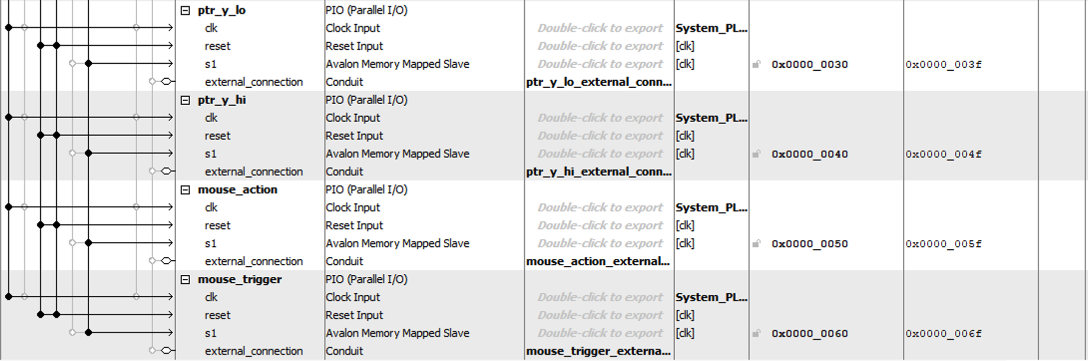
The software uses parallel input/output (PIO) ports to send information to the FPGA. There are 6 PIO signals:
ptr_x_lo, ptr_x_hi, ptr_y_lo, ptr_y_hi: these signals specify a square of the mouse selected area.-
mouse_action: this signal specifies which mouse button is active -
mouse_trigger: this signal is asserted high when any mouse button is being pressed
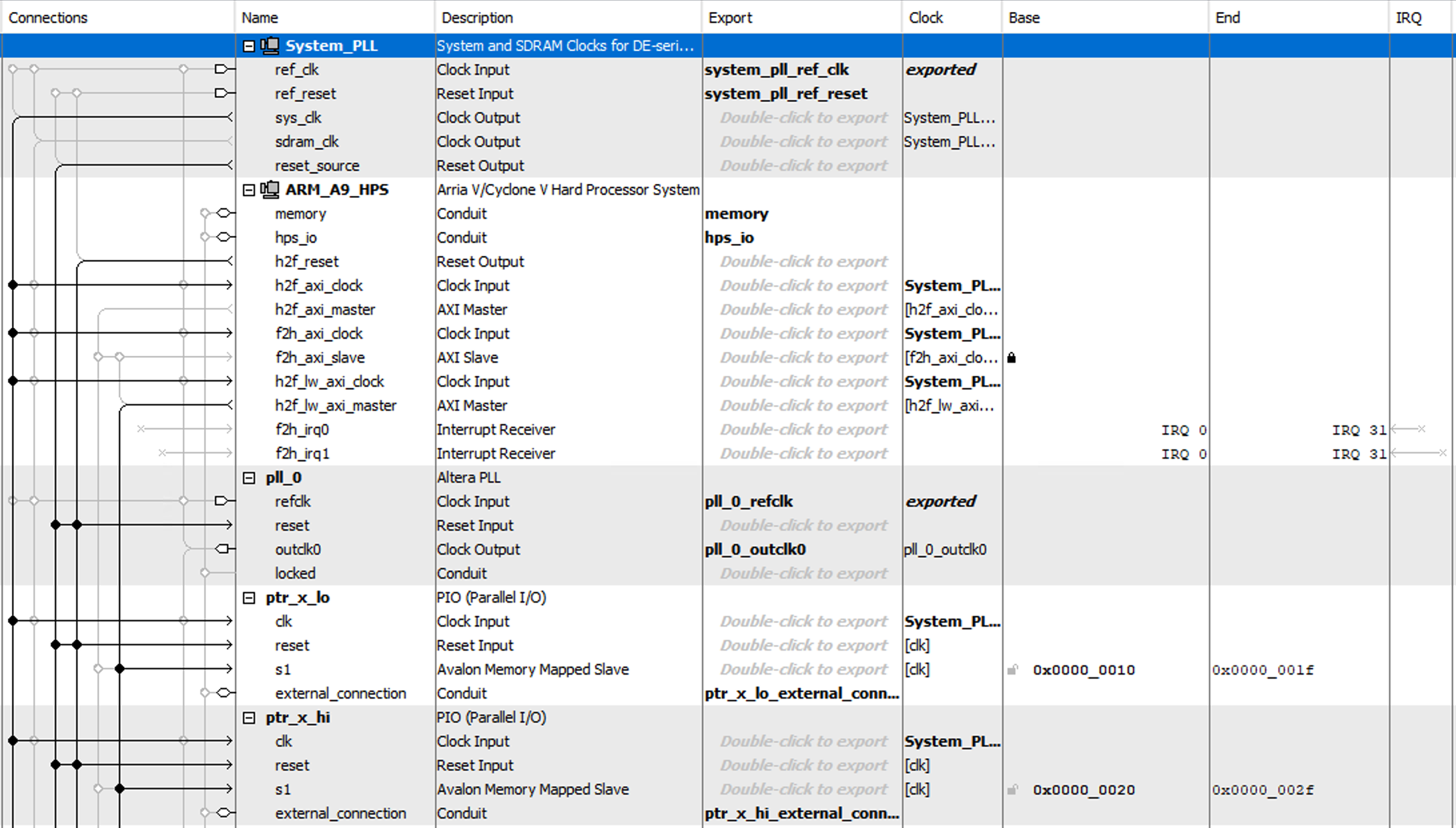
Here is the Qsys diagram
Mouse Input
Reading and parsing mouse input is straight-forward. We got a copy of the example code from this website. Changing the PIO signals given the mouse inputs is a trivial coding job.
Reference Code
Random Number Generation
We obtain and modify the random number generator from here. Bruce is the author.
USB Mouse
We obtain and modify the USB mouse parsing code from here. Bruce is the author.
VGA Driver
We obtain the modify the VGA driver from here. Hunter is the author.
Core Algorithm
We obtain the C copy of the core HPP algorithm from here. The author is honestly unknown.
Other RTL design is made in house
Things we thought about or tried but did not work
Here is a list of things that we have thought about or spent very little effort trying but did not work:
- Use 480 M10K blocks (each PE responsible for 1 row). This allows easier implementation but we simply don't have enough M10K blocks available on the board.
- Made particles visible to HPS. This will need very high bandwidth between the FPGA and the HPS. We have thought about it, but the methods we come up with will either slow down the framework or cause decoherency between the FPGA data and HPS's view.
- Use HPS to send arbitrary overwriting pattern to the FPGA. We want to do this and we think this is doable, but we simply didn't have enough time...