
Hardware (see Appendix for pictures and circuit schematics)
Each of the nodes on the HomeNet network perform similar tasks and, as such, there are many hardware components that they have in common. Each of the appliance nodes were made to be “standalone” so that they did not rely on any external components such as commercial development boards and were soldered to dispense with bulky breadboards.
Microcontroller Hardware
The most obvious common component of each node is the microcontroller itself. Each node on the network uses an Atmel Mega16L 8 MHz microcontroller to act as the “brains” for the network node. The microcontroller is responsible for coordinating communication across the RF network, providing timing to organize various tasks, and for providing control and functionality for the specific appliances on the network. Additionally, various other components are needed to support the microcontroller and to ensure correct operation. An 8 MHz crystal is connected to the microcontroller to provide an appropriate clock for the chip. Two 22pF capacitors are placed between ground and the clock pins to properly load the crystal so that it would produce a precise, regular clock signal. A 100 kΩ resistor connected the active low Reset pin to Vcc so that small transient charge buildups would not reset the microcontroller at undesired times. Also, the microcontroller is quite sensitive to noise and fluctuations on its power supply – even small changes in Vcc can also cause the microcontroller to reset. To combat this, a 0.1 μF capacitor is used to filter Vcc and ground to eliminate small, transient changes in the Vcc voltage. Six programming pins are also included in the circuit to make it very easy and convenient to reprogram the microcontroller even after it has been inserted into the circuit for the appliance node.
Power Supply
The Atmel Mega16L microcontrollers used require a steady 5V power supply to operate. Part of the design requirement for the nodes is that they are small and compact. This eliminates commercial 120V AC to 5V DC converts because they are too bulky to meet our design needs. Instead, we decided to use a 9V battery in conjunction with a voltage regulator to provide power for the network node. The voltage regulator chosen was the Analog Devices ADP3367 Linear Voltage Regulator. It was chosen because it can provide a stable 5V output for a variety of input voltages and has an extremely low quiescent current of 17 μA while still being able to supply 300 mA to drive the other components. The low quiescent current is desirable because it will extend battery life. The ability to accept a range of input is also desirable because as power is drained from the battery, the voltage the battery can supply will drop. Since the voltage regulator can accept input voltages as low as 5V, the life of a 9V battery can be extended beyond what is capable for other voltage regulators.
RF Transmitter and Receiver
Radio Frequency transmitters and receivers were chosen to allow wireless communication between nodes on the network. An RF communication scheme is ideal for the HomeNet platform because it is low cost and reliable over short ranges. The RF transmitters and receivers used are the Radiotronix RCR-433-AS and RCR-433-RP, respectively. These RF components are ideal because they are low cost, have low power consumption, and require no additional components other than a capacitor for filtering the power supply and an antenna, for better range. Additionally, the transmitters and receivers do all of the analog to digital conversion (and vice a versa) of data internally so there is no need for the microcontroller to interpret the signal. The transmitters and receivers can merely be attached to the transmit and receive pins of the microcontroller’s USART, so communication across the network is easy and seamless. The transmitters and receivers also comply with FCC regulations for unlicensed radio transmissions because they have a range of less than 300ft and operate at a frequency 433 MHz, which is in the unlicensed range. These Radiotronix components have a maximum data rate of 4800 baud, but we found that running them at the maximum rate caused a significant number of messages to be dropped. By halving the rate to 2400 baud we increased the reliability of the network by about 40% and also increased the maximum range that our nodes would operate at.
120V Control Circuitry
In the HomeNet system, the standard network node has the ability to control the flow of 120V AC wall power to the appliance plugged into the node. Working with 120V wall power presents several design challenges. Since the microcontroller and the rest of the circuit components run off a 5V power supply, they need to be kept completely separate from the 120V portion of the circuit. Not only is there the possibility of a short between the 5V side and the 120V side, but the 120V wall power would introduce significant noise even if all they shared was a common ground, which could cause the microcontroller to reset at inappropriate times. Not only is the node able to turn a light on and off, but it can also added dimming functionality to any standard incandescent lamp simply by plugging the lamp into the node. This is accomplished through the use of two separate circuits: a power control circuit and a zero crossing detector. In both of these circuits, optoisolators are used to keep the two sides separate yet still allow the microcontroller to interact with the 120V wall power.
The power control circuit is what allows the microcontroller to turn an appliance on and off. The two main components of this circuit are an optoisolator and a triac. For this circuit, a Fairchild Semiconductor MOC3011M optoisolator triac driver was used. The microcontroller side of the optoisolator consists of a light emitting diode with one terminal connected to Vcc through a resistor (to limit current flow) and the other terminal connected to a pin on the microcontroller. When the microcontroller sets the pin low, current is allowed to flow through the light emitting diode which begins to emit light. On the 120V AC side of the optoisolator, a light sensitive bilateral switch senses the incoming light and allows current to flow on its side as well. It is important to note that this implementation has no physical connection between the two sides; rather current flow is controlled by the transmission of photons. When the bilateral switch is enabled, the gate of a triac is connected to the “Hot” terminal of the 120V AC input. This activates the triac which allows current from the 120V input to flow between its two terminals. The triac chosen for this circuit is the On Semiconductor T2322B Sensitive Gate Triac. The T2322B was chosen because it is low cost, able to operate up to 200V and allows up to 2.5 A of current to flow, which is plenty to run normal household appliances.
This combination allows of optoisolator and triac allows the microcontroller to decide to allow current to flow to the appliance by setting its pin low, or to interrupt the flow by setting its pin high. It is important to note that the triac will not cut power off immediately when the bilateral switch is disabled. The triac will wait until a zero crossing occurs on the AC signal before disabling the 120V current flow. This prevents undesirable inductive spikes from occurring which could lead to significant noise or damage to the appliance.
The second circuit used for 120V power control is the zero crossing detector. This circuit is designed to raise a pin high on the microcontroller when the 120V AC signal crosses the 0V value. This is necessary to provide flicker-free dimming control to an incandescent lamp. Microcontroller regulated dimming is achieved by controlling the amount of power that is allowed to flow to the lamp.
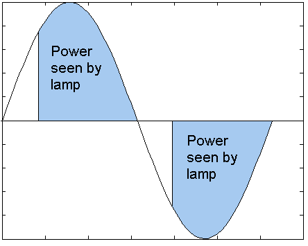
Figure 1 - Power passed for dimming
Given the sine wave of the AC signal, the area beneath the sine is effectively the power that is provided. The microcontroller can regulate the amount of power transmitted to the lamp by enabling the triac to pass current later in the cycle of the sign wave. By changing the interval between the zero crossing and when the triac is enabled, the microcontroller can effectively control the power flowing to the lamp. The amount of power passed is proportional to the intensity of light emitted by the lamp, so by reducing the power transmitted, the intensity of the light produced by the lamp is reduced. It is important for the microcontroller to keep the time interval after the zero crossing constant across cycles, otherwise the lamp will flicker rapidly and be uncomfortable to the human eye. It is therefore necessary for the microcontroller to know precisely when an AC zero crossing occurs.
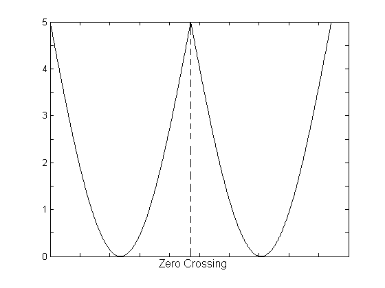
Figure 2 - Pin Voltage on Zero Crossing
The zero crossing detector circuit consists of two major components: a diode rectifier and an additional optoisolator. As far as dimming is concerned, the negative portion of the AC sine wave is treated identically to the positive portion. In order to be able to detect every zero crossing, it is necessary to take the absolute value of the sine wave. By using a diode rectifier, all negative values of the sine wave are converted to positive values and then fed into the optoisolator. After passing through the rectifier, the peak voltage of the AC signal is +50V. In order to limit the power dissipated by the optoisolator and prevent melting the component, the current flowing the optoisolator must be limited. Two 22 kΩ resistors were placed on the output of the rectifier to reduce the current flow to a manageable 1 mA. For this application a different optoisolator is needed. The MOC3011M used in the power control circuitry is designed for low voltage input to the light emitting diode and high voltage input to the bilateral switch. In the zero crossing detector circuitry, the opposite is needed. The NEC PS2501-1 was chosen to fit this need and the 1 mA input current was sufficient to activate the light emitting diode and enable the switch on the microcontroller side. One end of the switch is connected to ground and the other is connected in parallel to a resistor connected to Vcc and a pin on the microcontroller. When the AC signal approaches a zero crossing, the current passing through the light emitting diode drops and the switch is disabled, raising the pin of the microcontroller high. When the AC signal passes the crossing, current flows again and the pin is brought back to ground. So from the microcontroller side, whenever its pin is driven to a ‘1’, a zero crossing is occurring and it can take the appropriate measures.
Device Packaging
With the exception of the master node, all of the nodes were designed to be placed in a real home environment. Because of this, safety became an extremely important factor. The primary design for network nodes included the ability directly interrupt and control the 120 V RMS AC wall power, which means that potentially fatal electric shock could occur unless steps were taken to prevent it. The master node does not interface with any wall power appliance directly, so safety was not a major factor in its design.
In order to ensure that there was no possibility of accidental electric shock, there can be no exposed metal or portion of the circuit that is in contact with the wall power. To provide complete electrical insulation, we decided to use a bar sized travel soap box. Holes were cut in the lid of the soap box and a standard electrical outlet was mounted from the inside to allow any normal electric appliance to plug into our device directly. A separate three foot cord was used to connect our device to the wall outlet. The final soldered circuit, including microcontroller, battery, RF transmitters/receivers, and 120V control circuitry, was placed inside the plastic soap box and the entire unit was closed and sealed. This design allowed us to quickly and cheaply meet all of the safety requirements by allowing nothing to be exposed except the plastic portion of a standard electrical outlet, two small antennas, and the plastic casing of the soap box itself.
The decision to place the circuits within a small plastic enclosure, such as a soap box, made several other aspects of the design more challenging. Since the circuit is entirely enclosed, space is very limited and hence the design and layout of the hardware and circuit components had to be quite compact. Due to the large number of components used in the design, it was necessary to solder each circuit as compactly as possible, which was a time consuming and error prone task.
Master Node
In creating the prototype of the HomeNet system, it was decided that the master node would utilize the Atmel STK-500 development board. Using the STK-500 provided many benefits. The STK-500 is a well known commercial product that gave us a stable platform to use the microcontrollers with in the initial stages. It provides an easy interface with a PC for both programming and communication. Since the master node’s primary job is interfacing with the PC directly, and the network remotely, size and power supply was not a consideration. Additionally, the STK-500 has several built in push buttons and LEDs that were invaluable during the testing and debugging process.