![SW[9] to control the audio bus master](../DSP/Audio/Synthesis/Improved_string/disable_bus_master.PNG)
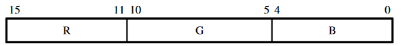
If R and B are 5-bit integers and G is a 6-bit integer then color = B+(G<<5)+(R<<11);
The following examples have been ported and verified in the Quartus Prime 18.1 version. So far, the only error messages were in Qsys Video modules. Two unused signals in the VGA_PLL module (which were dimmed) had invalid device names. The video_in_clock and LCD_clock have to be set to set to different device names, then unchecked again to disable them. Clearly a GUI error and easily fixed.
The projects that have been tested and ported to 18.1 are from material used in the assigned labs
and projects that exercise features of the FPGA and Qsys bus.
All of the examples will have a ZIP file containing the full Quartus project.
--
Download the zip file,
--
navigate to the Verilog folder
--
open the QPF file. This directly opens the project in Quartus 18.1.
-- When the project opens, the Quartus device programmer will find a valid SOF file to download.
-- DO NOT open the QAR archive! There is a bug in the archiver that eats Qsys designs.
Mandelbrot Set
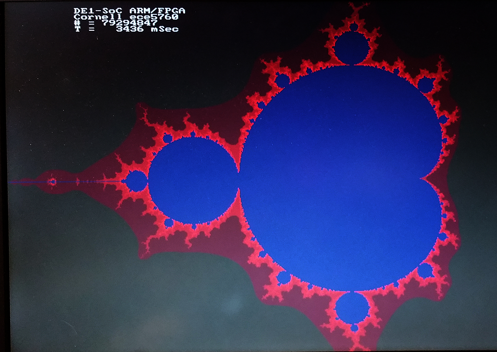
This example is a base-line implementation of a mandelbrot solver which displays using the DE1-SoC HPS computer system. It computes a 640x480 approximation with a maximum of 1000 iterations in about 933 milliseconds, using level -Os compiler optimization. The code computes about 80 million complex iterations/sec. To get this speed we converted the code to 4:28 fixed point arithmetic which lowers the time to 2.02 seconds, or about 39 million iterations/sec. Detecting circular regions of the slowest areas (in blue) and just setting the count to maximum in those regions lowers the drawing time to 0.93 seconds.
The colors are approximately logarithmic in number of iterations at that point. Image. The total number of iterations for all points on the screen and total execution time are displayed. Also included is a routine to erase all text on the screen. Use the sof file from the Zipped Quartus project without recompiling the project.
C code. ZIP project.
GPU with FAST display from SRAM.
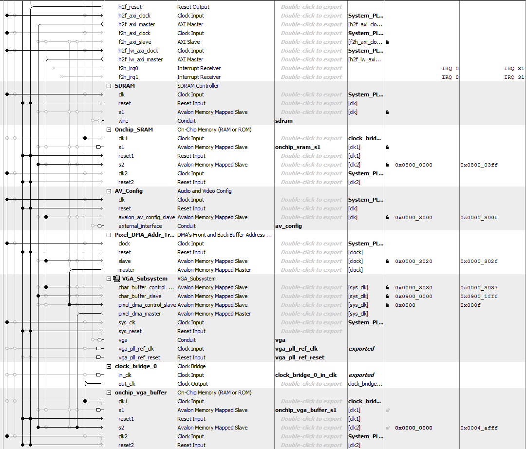
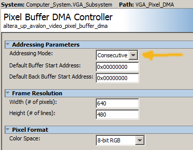
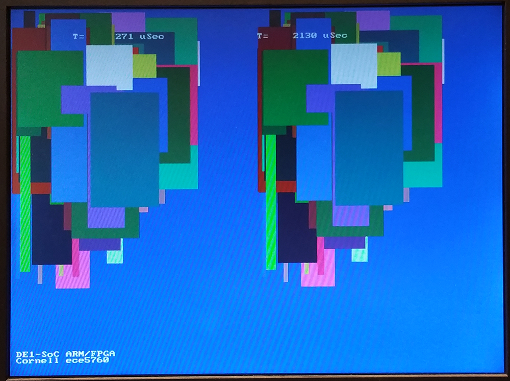
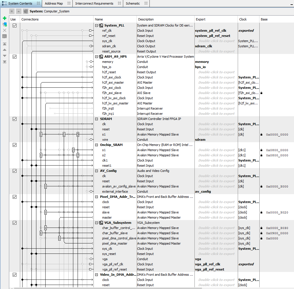
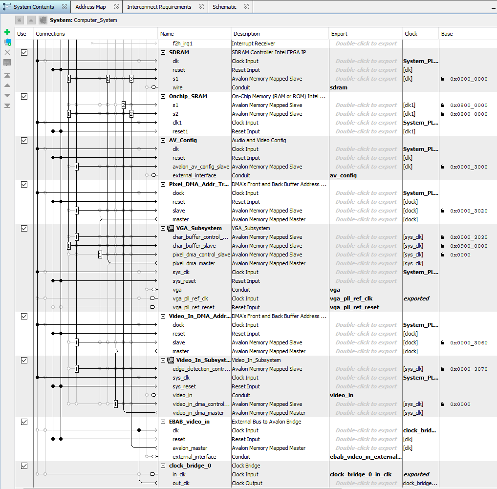
The write rate of the above SDRAM-buffered VGA is low, so I rewrote the system (Qsys layout) to use dual-port SRAM for the VGA buffer. One port (s2) is connected through Qsys to the VGA controller and HPS, as usual. The other port (s1) is exported to the FPGA fabric, and connected directly to the GPU state machine in Verilog. The clock bridge shown syncs the the SRAM slave port to the GPU state machine. The logic to control the GPU state machine from the HPS is unchanged from above. Direct connection of display memory to the GPU state machine results in a write-rate of 48 pixels/microsecond. To get the high rate, the GPU state machine was rewritten to pipeline writes to the VGA display SRAM. To minimize on-chip memory use, the display mode was set to 8-bit color and changed from x/y addressing to sequential addressing (video core section 2.1, code snippet), saving 30% of SRAM. To make the mode change, the VGA_pixel_DMA module dialog box in the VGA subsystem needs to be modified. The HPS code is also changed to reflect the modified display mode. The left and right sides of the screen are written respectively from hardware and from the HPS, and should match. The times at the top of the screen are the writing times of the last polygon for hardware and software respectively. (HPS code, top-level, ZIP). A slightly improved version of the HPS code does parameter validation before setting up the GPU draw operation. The SRAM display memory is bigger than the original, so use this address include file.
Audio output bus_master
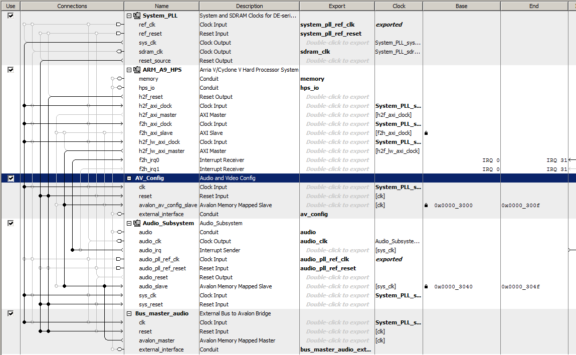
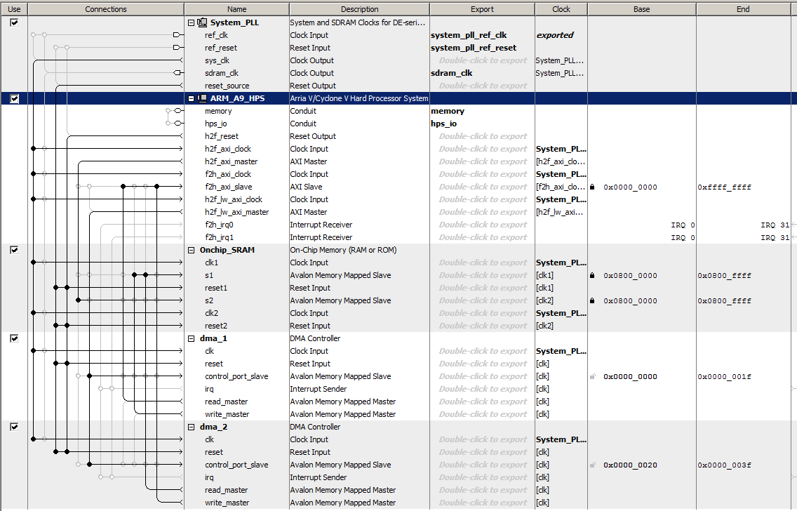
This bus_master state machine reads the FIFO status of the University Program audio interface, and if there is sufficient space in the FIFO, computes a new DDS sinewave sample and inserts it into the left and right audio channel FIFOs. The Qsys layout shows the relatively simple connections. The audio bus_master avalon_master is connected to the audio subsystem avalon_slave input. The design leaves the HPS interface in place, but contention between the two bus-masters for audio channels means that you can use one or the other (but see below for sharing the audio left/right channels). The state machine sets up the FIFO status read, then waits for the ACK. IF there is space in the FIFO, a new DDS sample is computed and written to the left channel, then waits for the ACK.
The right channel is then written. Both channels must be written for the audio interface to work. Waiting for space in the FIFO effectively phase-locks the state machine to the audio-rate clock for sound systhesis (top_level_module, project ZIP).
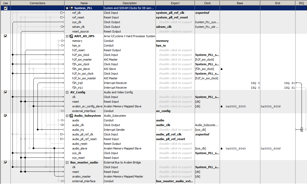
-- If the audio bus-master hardware only checks that status of the left channel FIFO and only loads the left channel FIFO, and the HPS only
checks that status of the right channel FIFO and only loads the right channel FIFO, then both can write to the audio at the same time. Since nothing is played by the audio interface unless there is data for each channel, the shorter duration channel determines play time. In this example, a WAV file is read by Matlab and samples sent by UDP to the HPS, which runs a thread to watch the UDP connection, and another thread to load the right channel. The hardware audio bus-master loads the left channel FIFO, then stalls until the HPS thread starts filling the right channel FIFO. (matlab program, HPS program, top-level module). The result is that the hardware plays a tone on the left channel during the time that the HPS program loads the right channel. Note that the hardware bus-master checks the top eight bits of the FIFO status word, while the HPS program checks the next eight bits (see section 4.1 of the Audio Core manual). The LEDR display is connected to the left channel FIFO status. When both sources are filling the FIFOs, you can see the contention by the variability of the FIFO depth, but actual audio play not affected.
Audio Synthesis of a Drum on HPS
The audio interface Verilog is converted to 16-bit sound, and the Verilog uses SW[9] to control the audio bus master to avoid conflict between samples produced by the HPS and Verilog audio bus master. Turn SW[9] ON to disable the bus master and allow the HPS exclusive control of the audio subsystem. When SW[9] is off, the bus master can control the audio interface. In this mode, SW[0] and SW[1] control filtering of audio signals fed into the line-input on the DE1-SoC, as described in Audio Filtering with decimated sample rate.
(Verilog, ZIP of quartus project, address_map_arm_brl4.h, Qsys layout).
A wave equation simulator on the HPS (drum code) supports a finite difference, second order scheme. The drum coded is a linear system with coefficients chosen so that cheap fixed-point shifts could be used to generate the 16-bit sound samples at 48Ksamples/sec. At -O3 optimization, I could just fit a 30x30 FDTD drum into the 20.8 microsecond systhesis time frame. If a more general drum tension is simulated with amplitude-dependent tension, then the size drops to about 24x24 grid points. See lab 2 (2019) for references and details. Courant stability puts limits on rho in the code (speed of sound) to 0<rho<0.5. A lower rho means lower natural frequency.
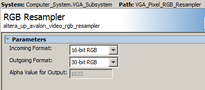
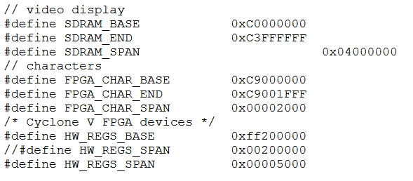
VGA video at 640x480 displayed from SDRAM, in 16-bit color.
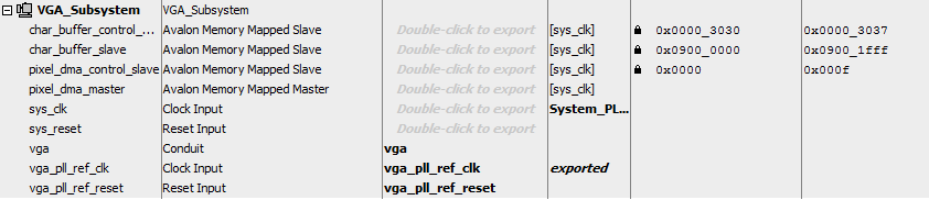
A stripped down display system uses SDRAM as a frame buffer.
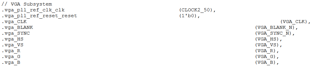
The top level Verilog only connects the Qsys exported signals to the i/o pins and has no other logic.
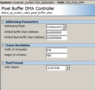
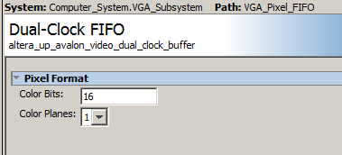
The Qsys layout is modified to support 16 bit color. The Qsys modifications:
The HPS pixel writing macro is modifed to allow 16-bit writes to the bus, and uses the consecutive format:
// pixel macro -- shift-left in the pixel pointer is specified in the Video Core Manual
// probably becuase the DMA addressing is all in bytes
#define VGA_PIXEL(x,y,color) do{\
int *pixel_ptr ;\
pixel_ptr = (int*)((char *)vga_pixel_ptr + (((y)*640+(x))<<1)) ; \
*(short *)pixel_ptr = (color);\
} while(0)
Defined graphics routines are
void VGA_text (int, int, char *); // (x_position 0-79, line_position 0-59, pointer_to_string)
void VGA_text_clear(); // clears whole text buffer, but not graphics
void VGA_box (int, int, int, int, short); // (corner1_x, corner1_y, corner2_x, corner2_y, color)
void VGA_line(int, int, int, int, short) ; // (point1_x, point1_y, point2_x, point2_y, color)
void VGA_disc (int, int, int, short); // (center_x, center_y, radius, color)
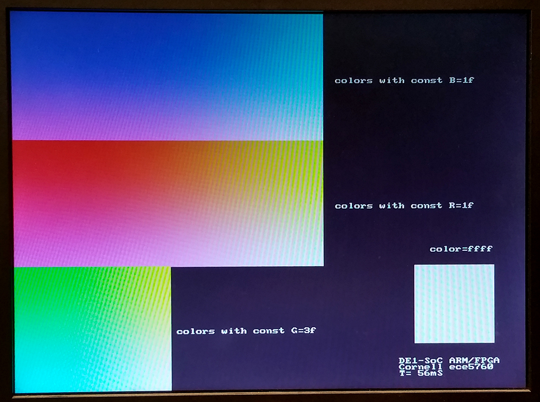
Color coding is 16-Bit RGB. This format uses 5 bits for red, and 6 bits for green and 5 bits for blue.
If R and B are 5-bit integers and G is a 6-bit integer then color = B+(G<<5)+(R<<11);
A color-picker program allows you to specify R, G, B values, displays the color in the lower right, and shows 2D slices through the 3D RGB space, axis aligned, which include the specifed (R,G,B) point. The top slice is the red-green plane, the middle is blue-green, and bottom is blue-red plane. Three examples are shown below through points black (0,0,0) , medium gray (15,31,15), and white (31,63,31).The HPS perfrormance program linked below prompts for color mask values to set ranges for RGB, then draws 1000 discs with random colors constrained by the RGB masks.


(HPS color picker, HPS performance measure, ZIP)
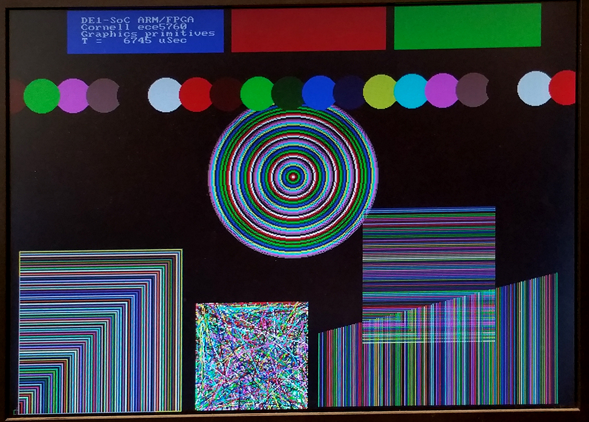
The graphics primitives were converted to 16-bit color (HPS program).
This program assumes the 16-bit hardware used above.
Bidirectional DMA to/from HPS
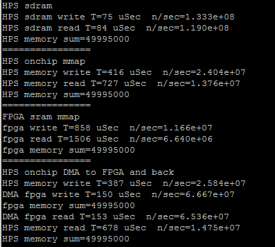
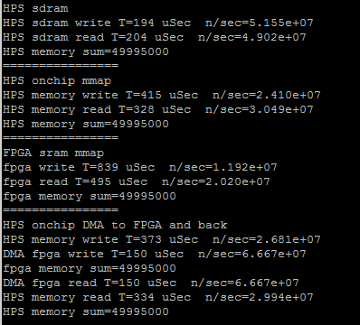
The Qsys was modified to include two DMA controllers connected so that data can be copied from HPS-to-FPGA and/or FPGA-to-HPS. The only connection differences are reversing the read and write bus-masters for the second DMA. (ZIP)
The HPS code was expanded to define the two DMA transfer controls, and to print the data transfer rates in each direction. The transfer rates are symmetric and both around 270 MBytes/sec. The rate limiting step is loading and reading the onchip RAM on the HPS. For 10000 32-bit transfers, the FPGA DMA read/writes each took 150 microceconds, but loading/reading the onchip memory took 730 and 550 microseconds respectively.
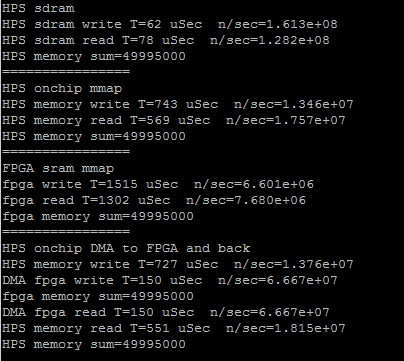
The next step in optimizing the HPS code is to replace the load/read loops with memcpy. Interesting to find out the memcpy is faster with no optimization turned on. The first image is from the program using memcpy compiled with -O3 option, the second with -O0. The direct read/write to SDRAM slows down. Also notice in the second screen dump that direct FPGA sram write takes 1330 microseconds. The DMA read/write takes 300 microseconds, but the overhead of loading the buffer makes the total about 1000 microseconds, not really much faster. (array of size 10000). The DMA transfer rate is about 270 MBytes/sec, but the net transfer rate (including data copy to buffer onship RAM) is about 77 MBytes/sec.
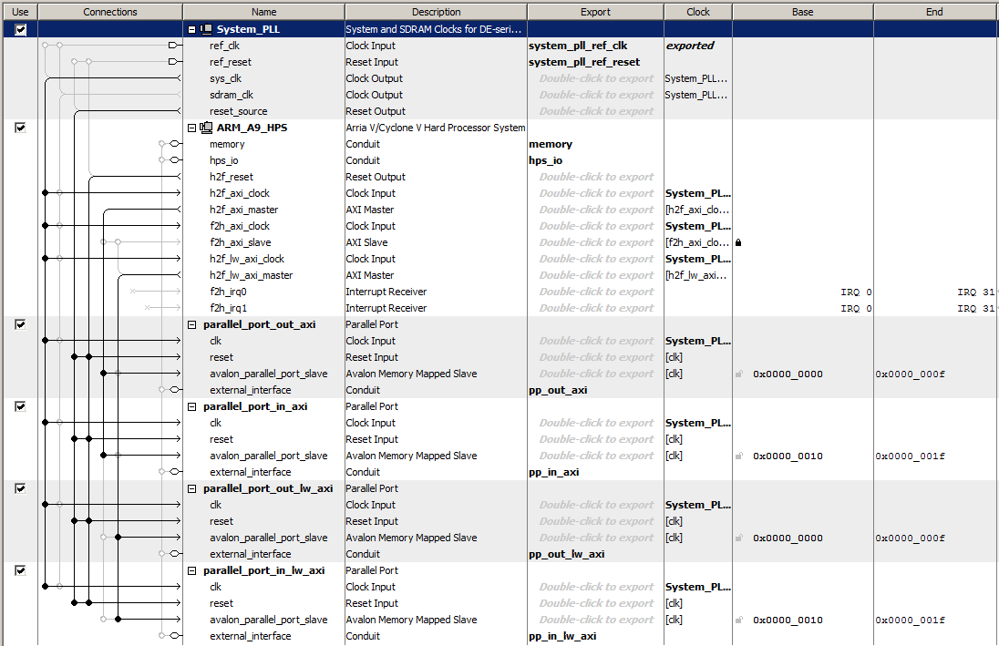
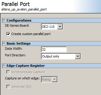
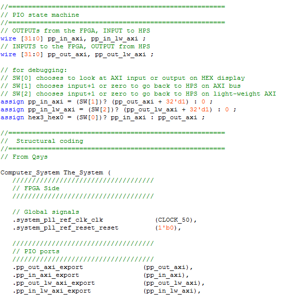
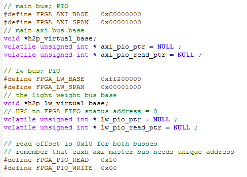
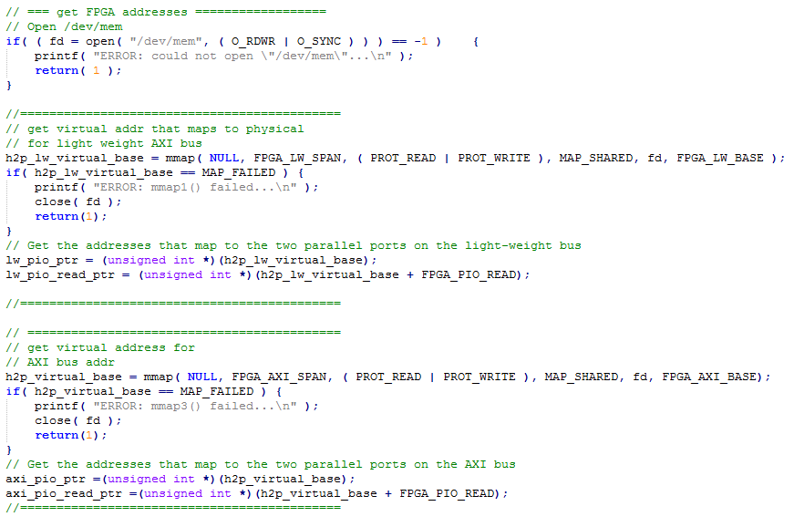
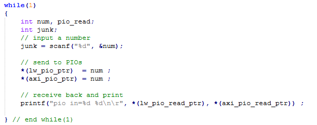
PIOs on AXI bus and on light-weight AXI bus
Parallel ports (PIO ports) instantiated in Qsys are defined as output if they communicate data from the HPS to the FPGA, and as input if then communicate data from the FPGA to the HPS. PIO ports can be instantiated on the light-weight AXI bus, or on the full AXI bus. This example instantiates four PIO ports in Qsys, one input/output pair on the light-weight bus and one i/o pair on the full AXI bus. As usual there will be Qsys, Verilog, and C involved in the setup
(C code, project ZIP) :
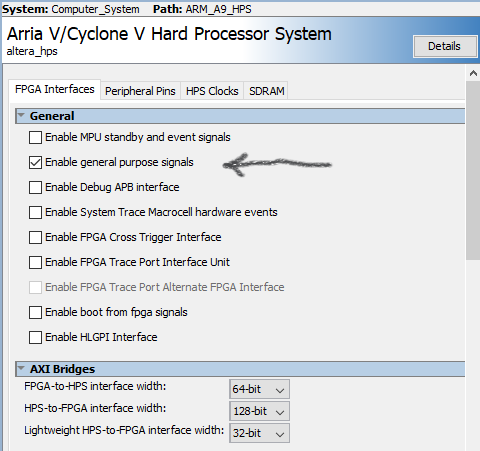
Direct I/O port from HPS to FPGA (not Qsys)
There
is one 32-bit input and one 32-bit output port from the HPS which can be directly connected to the FPGA fabric, with no Qsys address. To expose the i/o for connection, double-click on the ARM9_HPS component in Qsys, then in the dialog box click Enable general purpose signals. In the main Qsys window you should now see h2f_gp as a connection. Export it to form connections to FPGA. When you generate the new system, there will be signals:
// Direct gpio to FPGA
.arm_a9_hps_h2f_gp_gp_in (your_input_to HPS),
.arm_a9_hps_h2f_gp_gp_out (your_output_from_HPS),
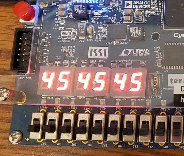
The example code displays:
AXI PIO input on Hex0
AXI PIO output on Hex1
The new gpio input on Hex2
The new gpio output on Hex3
LW_AXI input on Hex4
LW_AXI output on Hex5
For all three sets of i/o: input_value_to_HPS = output_value_from_HPS + 1
The serial interface allows you to enter a value to send to all three ports, and measures send/receive time for each of the three systems. The AXI bus is the fastest at about 6.5 million sends and receives per second. The LW_AXI is about half that speed, and the direct gpio port is about 5 million sends and receives per second. Since the signals are not on Qsys, it has it's own base address: 0xFF706000.
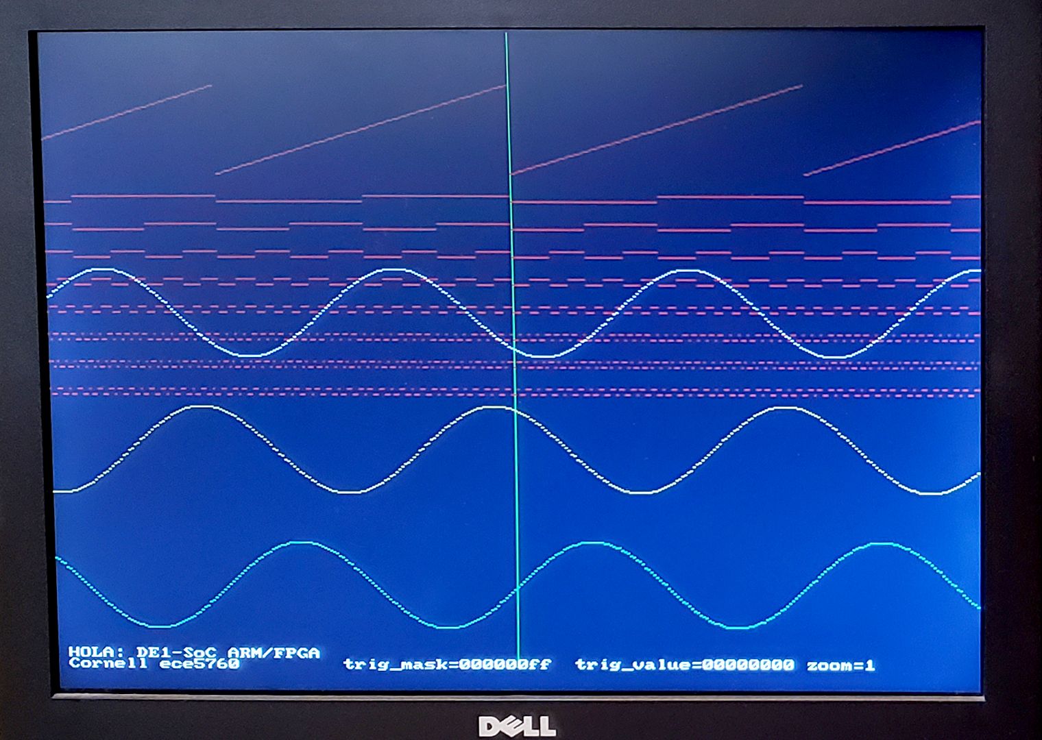
HOLA Homebrew Logic Analyser
Sometimes SignalTap feels like overkill.
I built a simple logic analyser that connects to one 32-bit data word and one 32-bit trigger word. If you start with the pre-built project and add your own device-under-test (DUT) , then the total programming overhead is to connect two 32-bit signals to your design. An example DUT is a three-phase DDS sinewave generator. The trigger mask is set to 0xff and the trigger word to zero, by the HPS. The green line is the trigger point. The 8-bit phase is plotted at the top. The bits of the phase are plotted in red. The three sine phases are plotted in green. The C functions for data handling are below.
C code, project ZIP, address map
Much more info on HOLA is available.
To make the system easier to use for debugging, the low level functions on the HPS were abstracted to five C functions:
Video Input with VGA output
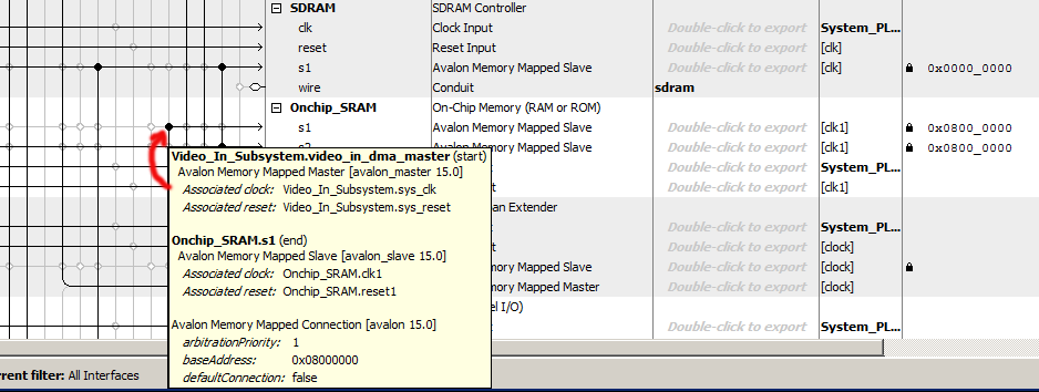
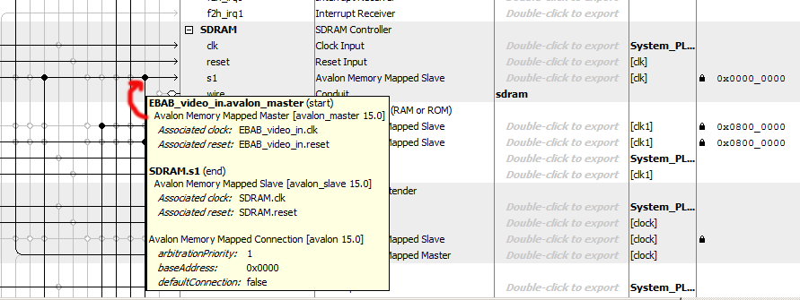
This example merges NTSC video input with VGA content generated by the HPS. Video input is stored in SRAM, then copied by a bus-master into VGA display SDRAM. The HPS initializes one feature of the video input, the just draws discs to the screen. The Qsys layout (part 1, part 2) adds a bus_master which can read from the on-chip SRAM used to store the video input and write to the VGA buffer SDRAM which is also connected to the VGA controller. The pixel copy state machine runs at 50 MHz, so a clock bridge was added to drive the the EBAB module. Video input is enabled by SW[1] up, Copy from the input buffer to the VGA display is enabled by SW[0] up, and you may need to turn both switches off and press KEY[0] to reset. A HPS progam must be run to set up the video input and demonstrate sumultaneous access to VGA from the HPS and custom bus_master. The VGA buffer bus traffic, plus video-input to VGA bus traffic, plus HPS to VGA bus traffic can exceed the bus bandwidth. The writing rate of the HPS program and the video-input to VGA are throttled. This version of the code has the screen position of the input image hard-coded, but the buffer can be resized and moved to other screen locations.
C-code, address header, Quartus ZIP file.
Example:

Implementing on-chip memory
On-chip memory can be built in several ways.
The different kinds of memory are confusing so we made an example that uses Qsys RAM, HDL-inferred M10k RAM, IP-manager RAM, and HDL-inferred MLAB blocks. The program reads two floats from the HPS, then sends them to Qsys RAM. There they are read then added or multiplied, and the result is read into M10k HDL infered memory and IP-manager M10k memory, then read back to Qsys RAM, which is read by the HPS. The Mlab blocks just read/write meory to make a little counting state machine. In addition, for sanity sake, the arithmetic results are also reported via 3 PIO ports.
There are some switched-based controls:
Observations:
References:
DE1-SOC literature list
Using the DE1-SOC FPGA by Ahmed Kamel
Stereoscopic Depth on an FPGA via OpenCL by Ahmed Kamel and Aashish Agarwal
Running Linux on DE1-SOC by MANISH PATEL and SYED TAHMID MAHBUB
OpenCL on DE1-SOC Sahil P Potnis (spp66@cornell.edu) Aashish Agarwal (aa2264@cornell.edu) Ahmed Kamel (ayk33@cornell.edu)
Audio Core (Qsys University Program 15.1) local copy
Video Core (Qsys University Program 15.1) local copy
Analog input Core (Qsys University Program 15.1) local copy
External to Avalon Bus Master (external here means in the FPGA, but not in the Qsys bus structure)
Avalon to External Bus Slave (external here means in the FPGA, but not in the Qsys bus structure)
Copyright Cornell University March 9, 2026